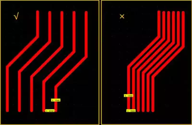
What is a PCB teardrop? A PCB teardrop is an additional copper pad, either straight or circular, located at the connection point between a pad or via and a trace, or when a trace transitions between different widths. For example, if part of your trace width changes from 10 mil to 4 mil, a teardrop is added at the transition point to reduce any stress or fine line cracking.
Types of PCB teardrops
One method (known as the ‘snowman’ method) involves adding auxiliary pads at the connection points between existing pads and traces. These auxiliary pads are smaller than the main pads and are centred a few mils away from the centre of the main pad.
Another more common method, known as rounded corners or straight lines, involves adding several traces from the existing pad to the existing trace.
The function of PCB teardrops
- Enhance mechanical strength
PCB Teardrops increase the contact area between the trace and the pad/via, dispersing external force impacts to prevent pad fractures or trace detachment, particularly in scenarios involving vibration or frequent insertion/removal. They prevent fractures at the pad or via connection points when the circuit board is subjected to external force impacts, especially during post-production repairs. When removing connectors, failing to add tear drops can easily cause the pad and trace to be torn apart together. Of course, this also depends on individual operational standards and is not absolute; it can only be said that adding tear drops is more advantageous! - Protecting pads
During multiple soldering processes, tear drops can buffer thermal stress, preventing pads from peeling off due to repeated heating, while also reducing cracks caused by uneven etching or via misalignment during production. - Smooth Impedance Transition
The PCB teardrop creates a smooth transition between the trace and the pad, reducing impedance jumps caused by sudden changes in trace width, thereby lowering signal reflection and attenuation. - Improve Production Yield Rate
During drilling, the PCB teardrop compensates for errors caused by drill bit drift or layer misalignment, preventing ‘breakthrough’ (where drilling deviation causes connection failure). - Aesthetic design
PCB teardrops create a more natural transition between traces and pads, enhancing the overall visual appeal of the PCB.
When are teardrops mandatory?
High-speed signal lines: DDR memory, high-speed serial buses (USB, PCIe, SATA, etc.) have extremely high requirements for impedance continuity, and teardrops can reduce signal distortion.
Risks of not using teardrops: Degraded signal integrity and worsened eye diagram quality.
High-current lines: Power lines and connections to power devices carry high currents, requiring sufficient current-carrying capacity at connection points.
Risks of not adding teardrops: Concentrated heat generation, which may cause connections to burn out over time.
Fine trace connections: When using narrow trace widths (e.g., <0.2mm) to connect pads/vias, mechanical strength is inherently insufficient.
Risks of not adding teardrops: Prone to breakage during production or maintenance.
Stress-prone locations: Board edge connectors, pads of components requiring insertion/removal, test points, etc.
Risk of not adding teardrops: Pads may peel off during insertion/removal or testing.
High-density board manufacturing process requirements: Some PCB manufacturers explicitly require the addition of teardrops to improve yield when etching precision is limited.
When can pcb teardrops be omitted?
Ultra-dense routing areas: Teardrops may encroach on adjacent trace space, exacerbating crosstalk; in such cases, prioritise maintaining routing spacing.
Solution: Disable teardrop functionality in specific areas.
RF/microwave circuits: Teardrop shapes may introduce small parasitic capacitance/inductance, affecting precise control of high-frequency performance.
Solution: Prioritise ensuring accurate impedance modelling; omit teardrops when necessary.
BGA bottom vias/pads: Teardrops may complicate solder mask openings and increase the risk of short circuits.
Solution: Teardrops are typically not added in BGA areas.
Standard low-speed, low-current digital signals: Teardrops may be omitted to simplify design when reliability requirements are not stringent.
How should teardrops be designed on a PCB?
Should pcb teardrops be thicker or thinner? You can refer to the manufacturer’s guidelines, which typically provide this information. However, as a general rule of thumb, you can use:
Vertex radius coefficient = ((PAD diameter – hole diameter)/1.8)
For through-holes with a small trace-to-pad ratio, drilling is critical. For military-grade dense boards, a ring-shaped circle should be retained around the through-hole
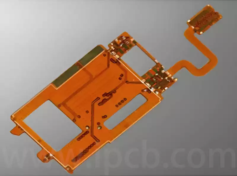
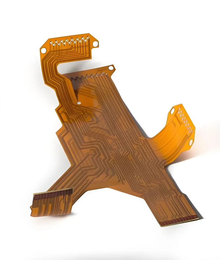
on flex-PCB layouts to reduce stress at the trace-to-pad connection.
Add teardrops under BGAs (with multiple vias), as shown in the figure below:
When traces leave the pad, teardrops should be added regardless of whether the pad is solid or has vias.
The importance of adding pcb teardrops increases as traces narrow.
Conductors wider than 20 mils do not require teardrops.
It is recommended to have the PCB layout include teardrops during the final design stage.
In some cases, this feature is simply a checkbox in the CAD system, which can be added directly in the CAD environment.
In RF or high-frequency boards, teardrops should be added during the design phase itself.
PCB manufacturers have teardrop creation engines.
When PCB manufacturers allow automatic teardrop creation, teardrop connections can be made to preserve DFM routes.
PCB teardrops are additional copper fillings at connection points, significantly enhancing mechanical strength, optimising signal transmission, and improving production yield. They are critical in high-speed, high-current, and stress-prone areas but may be omitted at discretion in certain high-density or RF applications. Designers should follow manufacturer guidelines and can utilise CAD tools to automatically complete teardrops during the later stages of PCB layout.