An SRAM chip, or Static Random Access Memory, is a type of memory that is capable of continuously storing data while the power supply is on. This type of memory is characterized by the fact that the stored data does not become invalid over time when the power supply is connected.
Application areas
- Computer systems
SRAM chips are often used as a cache in computer systems. They are integrated into CPUs and GPUs and take on the role of L1 and L2 caches, storing frequently accessed data and instructions, thus dramatically increasing computing performance. Since SRAM access speed is much higher than DRAM, it can effectively reduce processor waiting time and improve system efficiency. - Embedded System
In embedded systems,it is commonly used in microcontrollers. These chips provide enough storage capacity to support efficient data management and processing.SRAM is used as a cache in routers and other devices to realize fast data access and buffering functions. - Network Devices
SRAM is widely used in network devices such as routers and switches, mainly for storing routing tables and caching packets. These functions are critical for high-performance network systems that require fast access to stored information. - Consumer Electronics
SRAM chip also plays an important role in consumer electronics.For example, they help support multitasking in smartphones and provide faster data access compared to DRAM. SRAM is also often used in game consoles as a non-volatile cache to store runtime processing data. - Automotive Electronics
SRAM chip is also becoming more common in automotive electronics,especially in on-board computers and infotainment systems. They perform the key tasks of real-time data processing and information transfer to support advanced driver assistance systems (ADAS) and vehicle control units. - Industrial Control
In industrial control applications, SRAM is used as an important temporary storage solution to process signals and data to ensure real-time response and reliable operation of the system.This is especially important for industrial control systems that require fast read and write operations.
The SRAM chip operates on the basis of state switching of electrical crystals rather than capacitors to store data. As a result, it does not require periodic refresh operations like DRAM, which makes SRAM faster than DRAM in terms of speed.SRAM forms basic memory cells through a combination of transistors and resistors, and each cell can be accessed independently.
Manufacturing process
- Material Selection
The base material for SRAM chips is usually a silicon substrate. In the design, high-quality semiconductor materials are selected to improve electrical characteristics and reduce power consumption. For high frequency applications, new materials such as high mobility channel (HMC) may be used. - Transistor Design
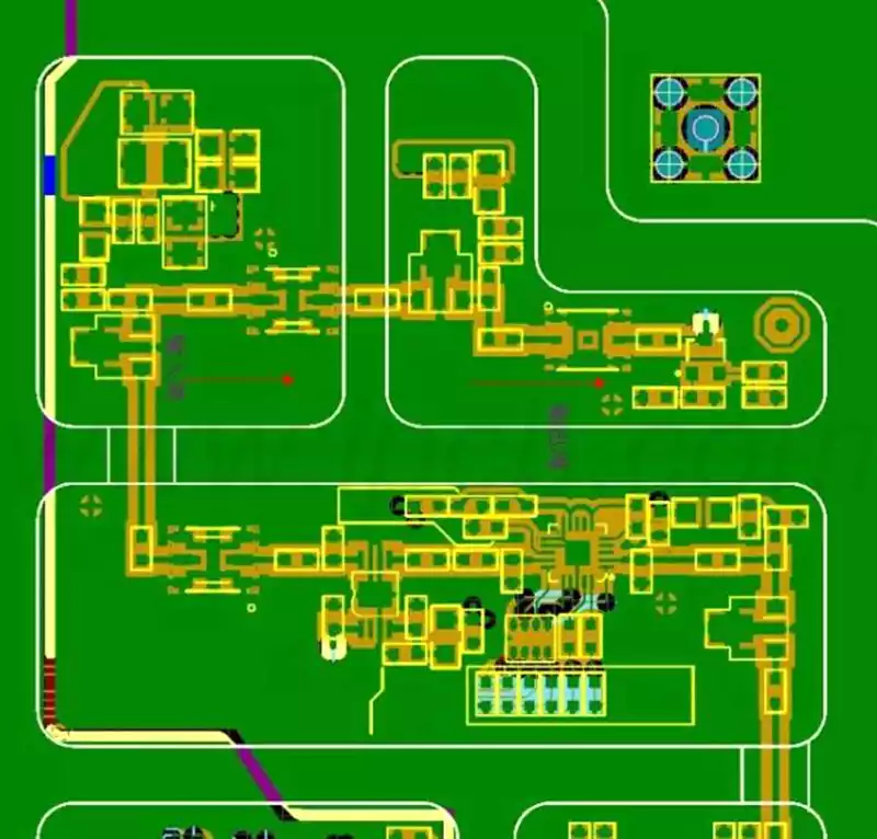
SRAM cells are generally composed of six MOS transistors (6T structure), where the number of pull-up transistors (PUs), pull-down transistors (PDs), and control switches (PGs) is usually set at 1:1:1 to ensure functional stability. However, the relative ratios of these transistors may be adjusted at design time in order to improve the static noise tolerance and write tolerance. Studies have shown that changing the quantitative relationship between PUs, PDs, and PGs affects the chip area and read/write stability of the SRAM cell. - The manufacturing process usually includes several key steps:
Photolithography: Patterned on a silicon wafer using photolithography to form a circuit structure.
Etching: Material not covered by a mask is removed by chemical or physical means to form desired trenches and other structures.
Epitaxial Growth: Growing layers of epitaxial material in specific areas, which is essential for building the structure of different transistors.
Metallization: Addition of metal layers at suitable locations to create electrical connections and form interconnects. - Process Control
Throughout the manufacturing process, it is critical to control the process parameters, including temperature, pressure and gas composition, to ensure process stability and consistency. For example, the use of asymmetric structure of the PG transistor manufacturing method can effectively improve the static noise tolerance and write tolerance of the SRAM, reducing power consumption. - Packaging and Testing
The fabricated SRAM chip must undergo rigorous testing to ensure that their functions are intact. After that, the chip will be packaged to protect its internal circuitry, especially in high temperature and vibration environments, to ensure its reliability.
Main features and advantages:
- High-speed performance
One of the biggest features of SRAM chips is their extremely high access speed. Since SRAM uses the same semiconductor process as CPU, the data access time is usually at the level of a few nanoseconds, which makes SRAM an irreplaceable position in the cache of computer processors. - No need to refresh
Compared with DRAM,SRAM does not require periodic refreshing of the circuitry to maintain the data stored internally. This feature not only simplifies the circuit design, but also improves the overall performance and efficiency of the system and reduces the dependence on the power supply. This makes SRAM perform better in applications with high real-time processing requirements. - High Reliability
SRAM has lower static power consumption and higher reliability, and can withstand higher voltage and temperature changes. This enables SRAM to work stably in complex and harsh environments, and is suitable for demanding applications such as automotive electronics and industrial control. - Unlimited Erase and Write Capability
SRAM chip is able to withstand unlimited data read and write operations, which gives them an obvious advantage in applications that require frequent data updates.In contrast,some other memories (such as EEPROM) are subject to the limitations of the number of writes. - Storage capacity and integration
Although the integration level of SRAM is relatively low and the storage capacity is usually smaller than that of DRAM, it can be used to design more complex storage structures to meet the needs of specific applications.SRAM chips are relatively large in size, so they are often used for small-capacity caches and special function modules.
With the rapid progress of information technology and artificial intelligence, the future development of SRAM (static random access memory) chip is facing multiple opportunities and challenges.SRAM chips in the future may develop several major trends:
- Increase storage density
Future SRAM designs will be dedicated to increasing storage density to meet the growing demand for computing. Driven by advanced process nodes (e.g., 5nm and below), researchers will explore new materials and design architectures to achieve higher transistor integration to enhance SRAM storage capacity . - Reduce Power Consumption
Low-power design will be an important direction for the future development of SRAM chips. As the concern for energy efficiency increases, chip designers will reduce the dynamic and static power consumption of SRAM through new materials and circuit architectures, such as the introduction of embedded storage and calculation technology, which combines the calculation and storage processes to achieve high energy efficiency. - Multi-chip integrated design
In the future, SRAM chips will more frequently use multi-chip integrated design (e.g., Chiplets), which integrates chips with different functions through high-bandwidth interconnects. This approach can, to a certain extent, overcome the limitations of a single SRAM chip in terms of storage density and power consumption, and combine a variety of storage technologies (e.g., SRAM and DRAM) to achieve more flexible storage solutions. - Supporting Emerging Application Areas
With the rapid development of emerging areas such as the Internet of Things (IoT) and Artificial Intelligence (AI), the demand for SRAM will continue to grow.SRAM is suitable for real-time needs to process massive data due to its high-speed and low-latency characteristics . As a result, SRAM chips are being optimized for these specific applications to support the needs of smart devices, edge computing, and data processing. - Software and hardware co-optimization
Future SRAM chip designs and applications will rely more on software and hardware co-optimization. Improved compilers and toolchains will ensure effective collaboration between hardware and application programs to improve SRAM usage efficiency and reduce power consumption. Such developments will help drive the use of SRAM in high-performance computing and artificial intelligence.
SRAM chip excel in speed and reliability, and is expected to further meet the needs of smart devices in the future by increasing storage density and reducing energy consumption. We expect it to continue to play a key role in the information technology field.