HDI step refers to the complexity of the manufacturing process of HDI boards, generally with the accumulation of layers (Build-up) to manufacture HDI boards, the more the number of layers, the higher the HDI process, the higher the technical grade of the board is also higher.
HDI order can be divided into the following categories.
HDI boards are divided into: 1st order, 2nd order, 3rd order, 4th order and arbitrary layer interconnections
1step HDI board: 1+N+1 (press fit 2 times, laser 1 time) is the most basic type of HDI board. It has the lowest number of connected lines but higher density. First-order HDI boards are mainly used for small electronic devices, such as cell phones and tablet PCs.
2 step HDI board: 2+N+2 (press fit 3 times, laser 2 times). Double-order HDI boards, is an additional layer of wiring on top of the first-order HDI board. This makes the number of connected lines on a second order HDI board double that of a first order HDI board, but still less than a third order HDI board. Second-order HDI boards are mainly used for medium-sized electronic devices, such as TVs and stereos.
3 step HDI structure: 3+N+3 (press fit 4 times, laser 3 times) Multi-order HDI boards are based on the 2nd order HDI boards with more layer lines added. This gives the third order HDI board the highest number of connected lines and the lowest density. Third-order HDI boards are mainly used for large electronic devices, such as automotive and aerospace.
4 step HDI structure: 4+N+4 (press fit 5 times, laser 4 times)
From the above structure can be summarized laser once for the 1st order board, twice for the 2 step hdi board, and so on. Of course, any layer interconnection is from the core board can already start radium, in the pressure before the need for radium is any layer interconnection HDI.
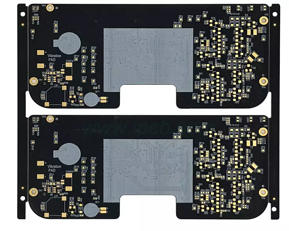
How to distinguish the first, second and third order of HDI PCB?
The first stage is relatively simple, and the process and technology are well controlled.The second stage becomes troublesome, one is the alignment problem, one is the hole punching and copper plating problem.There are various designs for the second order,one is that each order is staggered,and when it is necessary to connect the next neighboring layer,it is connected through wires in the middle layer,which is equivalent to two first-order HDIs.The second is that the holes of the two first-order layers overlap,so as to realize the second-order layer by superposition,and the process is similar to that of the two first-order layers,but there are a lot of process points that should be specially controlled,which is what is mentioned above.The third is directly from the outer layer of holes to the third layer (or N-2 layer),the process is much different from the previous,the difficulty of punching holes is also greater.For the third order to the second order analogous that is.
Examples are as follows:
6-layer board in the first order, the second order is for the need to laser drill holes in the board, that is, refers to the HDI board.
6 layers of first-order HDI board refers to blind holes: 1-2, 2-5, 5-6. That is, 1-2, 5-6 need laser drilling.
6 layers of second order HDI board means blind holes: 1-2,2-3,3-4,4-5,5-6. i.e. 2 laser drilling is required. First drill 3-4 buried holes, then press fit 2-5, then first drill 2-3, 4-5 laser holes, then press fit 1-6 for the second time, then drill 1-2, 5-6 laser holes for the second time. Finally the through holes are drilled. This shows that the second order HDI boards have been pressed twice and laser drilled twice.
In addition, the second-order HDI plate is also divided into: wrong hole second-order HDI plate and stacked hole second-order HDI plate,wrong hole second-order HDI plate refers to the blind holes 1-2 and 2-3 are staggered,while the stacked hole second-order HDI plate refers to the blind holes 1-2 and 2-3 are stacked together, for example: blind: 1-3, 3-4, 4-6.
And so on third order, fourth order …… All the same .
The number of times an order is pressed together.
First-order board, once pressed together that is, can be imagined as the most common boards
Second-order board,two presses, blind buried holes in the eight-layer board,for example,first do 2-7 layers of the board,press,this time 2-7 through-hole buried holes have been done,and then add 1 layer and 8 layers of the press up,playing 1-8 through-holes,made of the whole board.
3 step hdi pcb is more complex than the above, the first pressure 3-6 layers,plus 2 and 7 layers,and finally add 1 to 8 layers,a total of three times to press together, general manufacturers can not do.
Comparison of various orders of hdi boards
1 step HDI process: relatively low manufacturing cost due to the simplicity of the technology.
2 step HDI process: Manufacturing cost is higher than first order because more drilling,plating and lamination steps are required.
3 step HDI process: the highest manufacturing cost because it involves more complex process steps and high-end equipment.
HDI pcb is now widely used in cell phones, digital (camera) cameras, MP3, MP4, notebook computers, automotive electronics and other digital products,etc.,of which the application of cell phones is quite extensive. HDI boards are generally used in the accumulation of layers (Build-up) manufacturing,the more the number of times of accumulation of layers, the higher the technological grade of the board.Ordinary HDI board is basically 1 time layer,high-level HDI using 2 or more times the layer technology, while using stacked holes, plating to fill the holes, laser direct hole punching and other advanced PCB technology.High-order HDI boards are mainly used in 3G cell phones, digital video cameras, IC carrier boards and so on.
HDI process technology continues to evolve from first-order to high-order, not only enhancing the performance of electronic products, but also promoting the innovative development of the industry. With the continuous breakthroughs in technology, future electronic devices will be thinner, lighter and more efficient, leading the new trend of technological life.
