The printed circuit board (PCB) is an essential component in modern electronics, serving as the foundation upon which electronic circuits are constructed. Its development has been a journey of innovation, driven by the need for more efficient, reliable, and compact electronic devices. This article explores the rich history of the PCB, from its early conceptual stages to its present-day applications.
Early Beginnings of the printed circuit boards
The concept of a printed circuit can be traced back to the early 20th century. Before the advent of the Printed Circuit Board, electronic circuits were constructed using point-to-point wiring, which involved manually soldering wires and components together. This method was not only labor-intensive but also prone to errors and reliability issues. In 1903, German inventor Albert Hanson filed a patent for a method of creating flat, foil conductors on an insulating board. Hanson’s design involved the use of multiple layers of conductors separated by insulating layers, a concept that is still fundamental to modern PCBs. Although Hanson’s ideas were ahead of their time, they did not gain immediate traction.
Paul Eisler and the Birth of the Modern PCB
The breakthrough in PCB technology came in the 1930s with Austrian engineer Paul Eisler, who developed the first practical PCB while working in England. In 1936, he patented a method for printing conductive patterns on an insulating substrate using photoengraving. Eisler’s invention simplified circuit manufacturing and improved reliability. During World War II, the U.S. military adopted PCBs for proximity fuzes, enhancing artillery accuracy, marking the start of widespread PCB adoption in electronics.
Post-War Expansion
After the war, the use of PCBs expanded rapidly. The burgeoning consumer electronics market, driven by the demand for radios, televisions, and later, computers, spurred further innovations in PCB technology. In the 1950s, double-sided PCBs were developed, allowing for more complex circuits to be built on a single board. This advancement was followed by the introduction of multilayer PCBs in the 1960s, which further increased the density and functionality of electronic circuits.
The Advent of Surface Mount Technology (SMT)
The introduction of surface mount technology (SMT) in the 1980s was a major advancement in PCB technology. Before SMT, components were mounted through drilled holes and soldered on the opposite side. SMT allowed components to be mounted directly onto the board’s surface, reducing the size and weight of devices while improving performance and reliability. It also enabled automated PCB assembly, leading to faster production and lower costs. SMT’s miniaturization was crucial for modern consumer electronics like personal computers and mobile phones.
Manufacturing Processes of the printed circuit board
The manufacturing of PCBs involves several key processes, each of which has evolved significantly over the years:
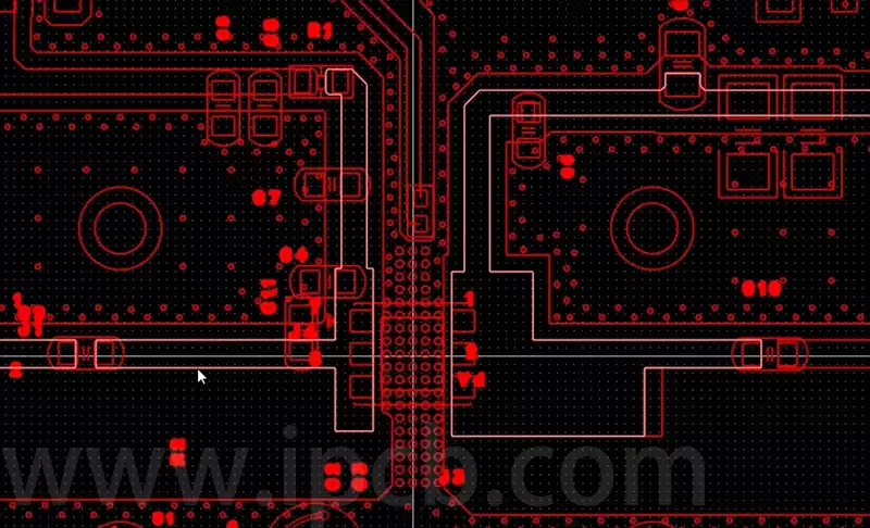
- Design: The process begins with the design of the circuit, typically using computer-aided design (CAD) software. The design specifies the layout of the conductive traces, component placements, and other critical features.
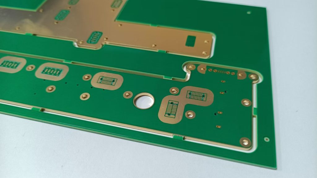
- Material Selection: The substrate, or base material, of the PCB is usually made of fiberglass-reinforced epoxy resin, known as FR-4. Other materials, such as flexible polymers, may be used for specialized applications.
- Patterning: The conductive pattern is created using a photoengraving process. A layer of copper is applied to the substrate, and a photosensitive film is used to transfer the design onto the copper. The exposed copper is then etched away, leaving the desired pattern.
- Drilling: Holes for through-hole components and vias (connections between different layers) are drilled into the board.
- Plating and Solder Mask Application: The drilled holes are plated with copper to create electrical connections. A solder mask is then applied to protect the conductive traces and prevent solder bridges during component assembly.
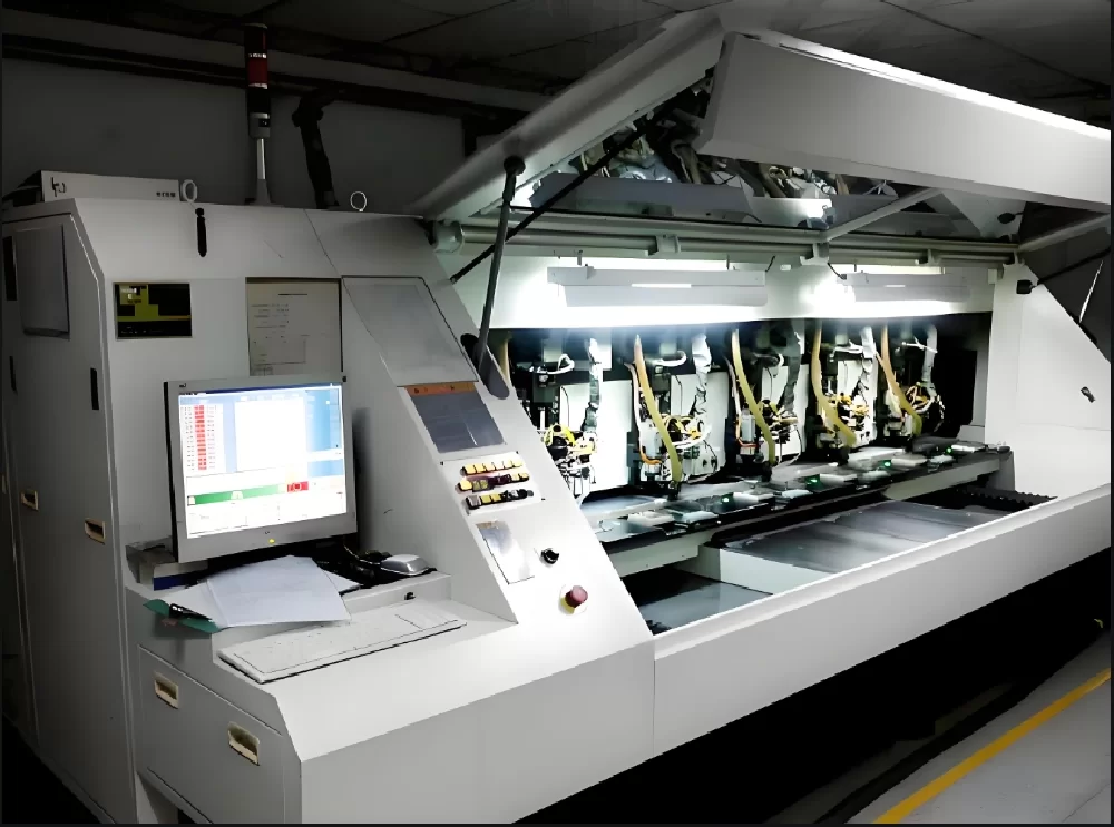
- Component Assembly: Components are placed onto the PCB using automated machines. For SMT, components are placed directly onto the board, while through-hole components are inserted into drilled holes.
- Soldering: The components are soldered to the board using reflow soldering (for SMT) or wave soldering (for through-hole components).
- Testing and Inspection: The assembled PCB undergoes rigorous testing and inspection to ensure functionality and quality. Automated optical inspection (AOI) and X-ray inspection are commonly used techniques.
Advancements in the printed circuit board Technology
The evolution of PCB technology has continued into the 21st century, driven by the demand for smaller, faster, and more efficient electronic devices. Some of the key advancements include:
- High-Density Interconnect (HDI) PCBs: HDI technology allows for the creation of PCBs with very fine features, enabling higher component densities and more complex designs. HDI PCBs are essential for modern smartphones, tablets, and other compact devices.
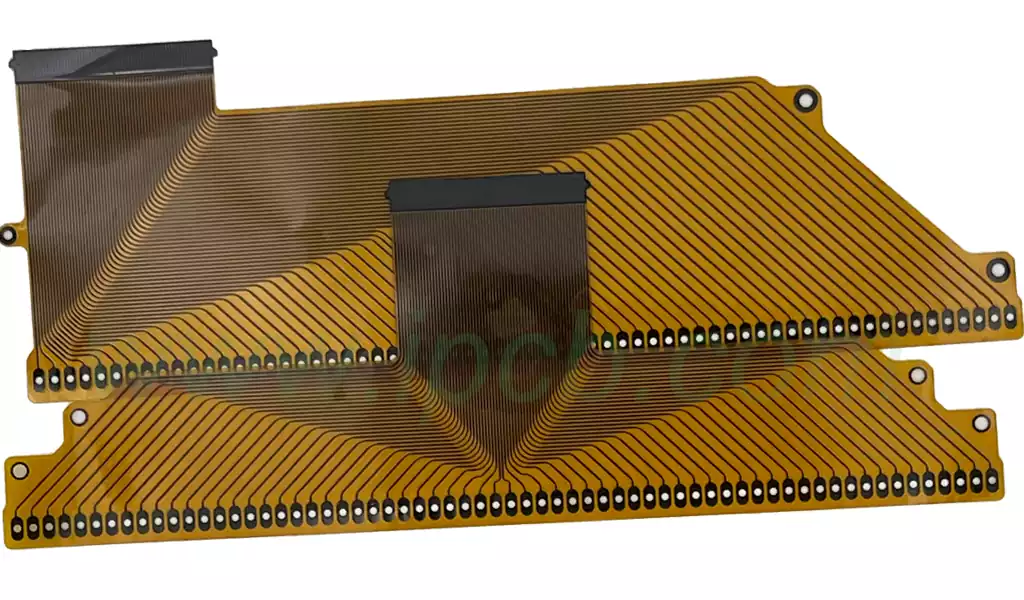
- Flexible and Rigid-Flex PCBs: Flexible PCBs use flexible materials that can bend and twist, making them ideal for applications where space and weight are critical. Rigid-flex PCBs combine both rigid and flexible sections, offering greater design versatility.
- Embedded Components: Advances in PCB manufacturing have made it possible to embed passive and active components within the layers of the board, reducing the overall size and improving performance.
- Environmental Considerations: The electronics industry has become increasingly focused on sustainability. Lead-free soldering, the use of environmentally friendly materials, and improved recycling methods are now standard practices in PCB manufacturing.
The Future of the printed circuit board
The future of PCB technology is likely to be shaped by several emerging trends and innovations. Some of the most promising developments include:
- Printed Electronics: The use of conductive inks and printing techniques to create electronic circuits on various substrates is an area of active research. Printed electronics have the potential to revolutionize manufacturing by enabling low-cost, large-area, and flexible circuits.
- 3D Printing: 3D printing technology is being explored for the production of PCBs with complex geometries and integrated components. This approach could lead to new design possibilities and faster prototyping.
- Wearable and Implantable Electronics: The demand for wearable devices and medical implants is driving the development of ultra-flexible and biocompatible PCBs. These applications require materials and manufacturing processes that can withstand the unique challenges of the human body.
- Artificial Intelligence and Machine Learning: AI and machine learning are being used to optimize PCB design, manufacturing, and testing processes. These technologies can help identify defects, improve yield, and reduce development time.
The history of the printed circuit board is a testament to human ingenuity and the relentless pursuit of technological advancement. From its humble beginnings as a solution to the limitations of point-to-point wiring, the PCB has evolved into a cornerstone of modern electronics. As we look to the future, continued innovations in PCB technology will undoubtedly play a crucial role in shaping the next generation of electronic devices, driving progress in fields as diverse as consumer electronics, healthcare, and beyond.