In the field of modern electronics manufacturing, SMT (surface mount technology) and burn in board is inextricably linked, and their synergistic effect is a key link to ensure the stability and reliability of electronic product performance.SMT technology, as the basic process for manufacturing aging boards, enhances the durability and accuracy of burn in boards in the extreme test environment through high-precision component mounting and advanced welding processes, thus laying a solid foundation for the performance verification of semiconductor and electronic products. electronic products, thus laying a solid foundation for the performance verification of semiconductor and electronic products.
SMT (Surface Mount Technology), as a key process for surface mounted components, has become an important support for the production of burn in boards with its high precision and efficiency.
(1) Miniaturised design and high-density layout
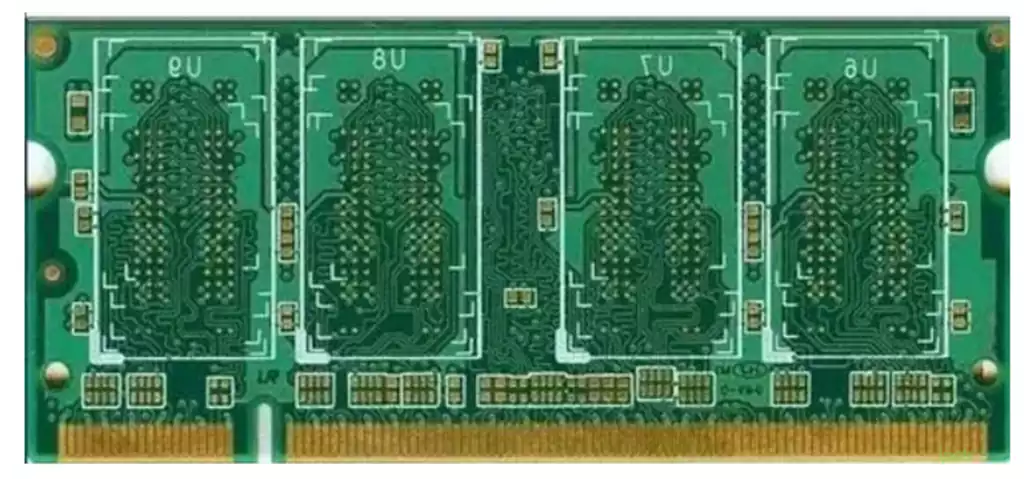
Test boards and burn in boards are often integrated with a variety of complex circuit modules, including signal conditioning, high-speed interfaces and power management, etc., the density of the layout of the components have very high requirements, SMT technology can achieve 0201 (size 0.6 × 0.3mm) level of tiny components mounted, and with the help of multi-layer PCB design to achieve a dense line wiring. For example, in the semiconductor test board, SMT chip technology supports high-precision ADC / DAC chip quickly installed to meet the needs of high-frequency signal acquisition and analysis.
(2) Reliability guarantee and precision welding
Test board and burn in board electrical performance on the accuracy of the test results play a decisive role in the SMT process using multi-temperature reflow soldering technology, precise control of preheating, constant temperature, reflow and cooling process temperature curve (peak temperature is generally 240-260 ℃), to ensure that the solder joints to form a uniform eutectic structure, to prevent the emergence of false soldering, bridging and other defects. At the same time, combined with automatic optical inspection (AOI) and X-ray inspection technology, real-time monitoring of the quality of the solder joints to ensure the long-term stability of the test board and aging board performance.
(3) Mixed assembly to meet diversified needs
Some test boards and burn in board needs to be compatible with SMT chip components and THT plug-in components (such as high-power inductors and connectors, etc.), the use of SMT and THT hybrid assembly process not only to meet the needs of high-density layout, but also take into account the mechanical strength, especially suitable for industrial-grade or automotive electronics test environment. Taking high-power semiconductor test boards as an example, SMT is responsible for the placement of high-density signal processing modules, while THT takes on the task of installing power devices with high heat dissipation requirements.
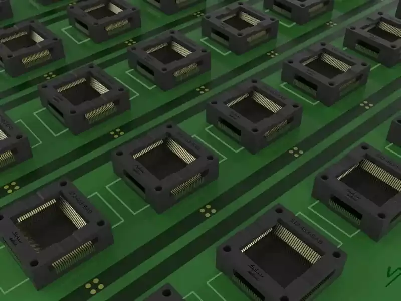
Burn in board is an important tool in the reliability testing of electronic products by simulating the accelerated aging process of electronic components in high temperature environments (usually over 80 degrees Celsius) with humidity of 85% or more. It utilises extreme high voltage and thermal stress to rapidly expose potential early failures and hidden dangers of products to ensure stable performance and extended life in the actual use environment. The harshness of the aging test environment makes it necessary for the burn in board to have extremely strong thermal resistance and structural stability, and any minor material defects or poor welding will directly affect the accuracy of the test, which in turn affects the quality assurance of the subsequent products.
In response to the special operational needs of the burn in board, SMT technology in the material and process to make a breakthrough in various aspects. The use of high glass transition temperature (Tg) substrates has become a key, the Tg value of such substrates can reach 170 degrees Celsius or higher, which greatly improves the board’s ability to resist deformation and performance degradation in continuous thermal cycling. Compared to traditional FR-4 materials with lower Tg, high Tg substrates show better mechanical stability during repeated thermal expansion and contraction, avoiding the risk of loose or broken solder joints due to the softness of the substrate.
The choice of solder paste is particularly important, the use of lead-free solder paste with excellent high-temperature performance, able to withstand the reflow soldering process 240 to 260 degrees Celsius peak temperature, and to ensure that the solder joints in a number of high-temperature cycling is still maintained after good mechanical strength. Such a solder material in the actual application of the solder joints significantly reduced due to thermal fatigue cracks and false soldering, the actual data of some cooperative manufacturers, through the improvement of the solder paste formula, its product rework rate reduced by about 20%.
The precision placement capability of SMT technology also significantly improves the performance of aging boards, and the use of laser selective soldering technology to accurately reinforce solder joints strengthens the thermal cycling resilience of critical signal pathways on the board. In the 0.4 mm pitch BGA chip placement, micron-level positioning accuracy ensures signal quality, and test results show that signal insertion loss is controlled within 0.5dB/10GHz, meeting the demands of high-speed and high-frequency applications. This is especially critical for highly complex electronic products such as 5G communication modules, where stable signal transmission directly affects device performance and user experience.
The integration of SMT technology and burn in board
The deep integration of SMT and burn in test boards has given rise to three major directions of technological breakthroughs:
Heterogeneous integration capability
Through laser-assisted bonding technology, heterogeneous integration of chips, MEMS sensors, and passive components is achieved. The integrated test board developed by a research institute has successfully reduced the aging test time of sensor modules by 70%.
Intelligent Production Line Upgrade
The integration of digital twin technology enables virtual debugging and real-time optimisation of aging test board production lines. According to an automation manufacturer, the intelligent production line has improved the CPK of test boards to 1.67.
Material Science Breakthroughs
Development of low-temperature soldering materials (e.g., nano-silver paste) to reduce reflow soldering temperature to below 180°C. This technology enables the flex life of flexible electronic test boards to exceed 100,000 bending cycles, expanding wearable device testing scenarios.
SMT technology, as the core driver of burn in board manufacturing, effectively improves the performance and durability of aging boards in extreme testing environments with its ultra-high precision, high-density layout and reliability guarantee.