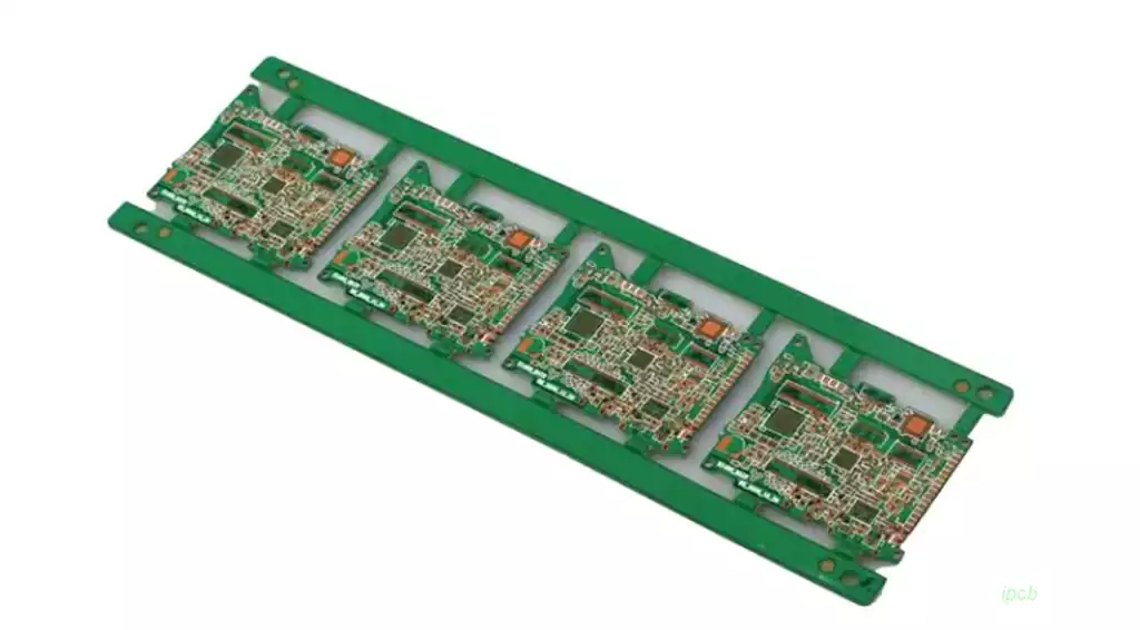
PCB blind via buried via technology realizes the precise connection between the inner layer of the circuit board and the surface layer of the circuit board with the help of a unique processing technology. This technology not only significantly increases the density of the circuit board wiring, but also effectively enhances the overall performance and stability of the circuit board. Blind and buried vias, as important components of the blind and buried vias process, each play a key role. Blind vias specialize in the connection between the inner layer and the surface layer, while buried vias focus on the interconnection between the inner layer. Working in tandem, the PCB blind vias have revolutionized electronics manufacturing.
PCB blind buried vias process is aimed at high-density multilayer PCB manufacturing, circuit board layers, the line is difficult to go through the problem and the development of. The process can realize the internal interconnection of the PCB board, improve the integration and performance of the circuit board, so that PCB designers can arrange more lines in a smaller space, to achieve a higher circuit density. Currently, blind buried hole technology has become one of the core technologies in the manufacture of high-density multilayer printed circuit boards.
Buried vias are a way of connecting signals or currents from one inner layer to another by setting up vias that connect the inner layer alignments. It is very common in multilayer PCB design. By setting up buried vias in the design, complex inner layer alignment layouts can be effectively organized.
Blind vias are a type of via that connects inner layer alignments to surface layer alignments. Blind vias have more complex process requirements and higher manufacturing costs than buried vias, but in some specific design requirements, blind vias can provide greater layout flexibility and circuit performance.
Process Differences
There are some significant differences between buried vias and blind vias in the PCB manufacturing process. Buried vias are relatively simple to process and can be realized through traditional processes such as mechanical boring. Blind vias require more complex drilling and blind hole copper plating technology to realize the inner layer of the alignment and the surface layer of the alignment of the connection. In addition, blind holes are more demanding and require special blind hole drilling machines for accurate positioning and drilling of the inner layer. Buried holes, on the other hand, do not require high precision and can be processed by conventional mechanical drilling. Blind vias is also relatively expensive to manufacture, including the investment in drilling and copper plating of the blind holes. The cost of buried holes is relatively low, which can effectively reduce the overall manufacturing cost.
Comparison of the advantages of blind buried vias
Advantages of blind vias:
Optimized PCB structure
Blind vias are designed so that the structure of the PCB board is optimized. This hole structure is drilled from one side of the board to a specific depth and then stops, and unlike perforations, it does not penetrate to the other side of the board. This design not only reduces the number of circuit layers, but also reduces the thickness of the board, which is particularly suitable for small electronic devices.
Reduced Production Costs
Since blind vias only need to be drilled to a specific depth from one side of the board, they have a lower wall height than perforated holes. As a result, blind vias are simpler to process and more efficient to produce, thereby reducing PCB manufacturing costs. Blind vias are also relatively easy to open, align, and lithograph, further reducing costs.
Improved Reliability
Blind vias are simple and inexpensive to process, and can significantly improve the reliability of circuit board. Blind vias effectively avoid possible defects inside the perforation, preventing wires from creeping and ensuring circuit stability and accuracy. This means that blind vias provide better performance when dealing with high intensity or peak operating signals.
Benefits of buried vias:
Facilitates High-Density PCB Integration
The design of buried vias meets the PCB’s need for high-density integration, effectively saving line space and providing strong support for board miniaturization.
Enhance PCB strength
The hole wall design of buried holes avoids visible bumps, which improves the overall strength and stability of the PCB. This design reduces the risk of stress-induced cracks and scratches, enhancing the durability of the PCB.
Prevents circuit short-circuiting and leakage
During the PCB manufacturing process, the connection between components and deep circuits is often prone to short-circuit and leakage problems. The presence of buried holes can effectively prevent these problems and ensure the stable operation of circuits. The design of buried holes makes the circuit layout more reasonable and reduces potential safety hazards.
PCB blind buried vias process:
According to the specific design requirements of the PCB, first of all, the specific location and number of blind and buried holes, and rational planning of its layout to ensure that it meets the needs of the circuit connection.
Produce images of the inner layer alignment and surface layer alignment to form a copper foil graphic template. On this basis, the positional information of blind and buried holes is accurately incorporated to provide precise guidance for subsequent processing operations.
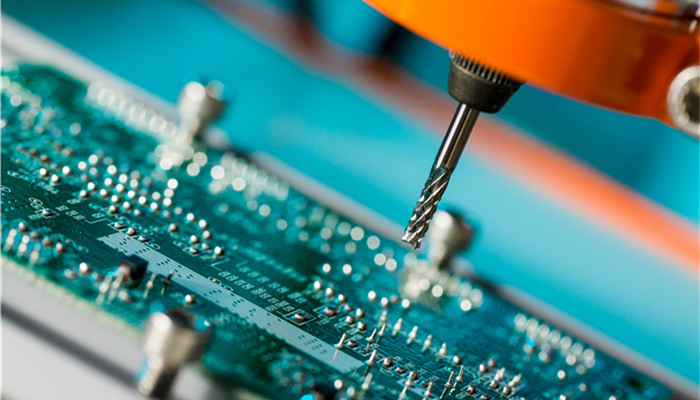
In accordance with the design requirements, advanced laser or mechanical drilling technology is used to accurately drill blind and buried holes on the PCB board to ensure that the location, size and depth of the holes meet the design requirements.
In order to improve the conductivity of blind and buried holes, special treatment of the hole wall is required. Common treatments include chemical copper plating and electrolytic copper plating, etc., through which the conductive ability of the hole wall can be effectively enhanced.
Covering the walls of blind and buried holes with a soldermask or conductive layer to prevent short-circuiting between the inner alignment and the blind and buried holes. This step is critical to ensure the stability and safety of the board.
In order to enhance the protective properties of the PCB and improve its appearance, an outer copper cover and board surface treatment is required. This step can ensure that the board has better durability and aesthetics to meet the needs of practical applications.
Caution:
PCB blind buried hole process in practice need to pay attention to the following points:
The location and number of blind and buried holes should be reasonably planned according to the circuit design requirements to ensure the reliability and performance of the circuit connection.
The accuracy of drilling and the flatness of the hole wall is critical to the quality of blind-embedded holes, which requires the selection of appropriate processing equipment and process technology.
The treatment of the hole wall should be based on the PCB material and the actual situation to choose the appropriate chemical copper plating or electrolytic copper plating process to ensure the conductivity of the blind and buried holes.
In soldermask covering and baking, temperature and time need to be controlled to ensure the quality of the soldermask layer and to avoid quality problems such as short circuits.
In the outer layer of copper cover and board surface treatment, it is necessary to use the appropriate process and materials to take into account the protection performance and appearance effect.
PCB blind via buried via technology, as the core process of high-density multilayer PCB manufacturing, not only improves the circuit board wiring density and performance, but also in the field of electronic manufacturing has brought about a revolutionary change. With the progress of science and technology and the growing demand for electronic products, they will continue to play an important role in promoting the field of electronic manufacturing to the direction of higher density, higher performance.