The dielectric constant is an indicator of a material’s capacitive properties in an electric field, and it measures a material’s ability to store charge in an electric field. For PCB boards, the pcb dielectric constant DK value reflects the capacitance capability of the insulating layer of the board and is used to define the electrical properties of the board. Different boards have different dielectric constants, common PCB boards such as FR4, ROGERS, PPE, etc., its dielectric constant DK value is generally between 2.5~5.
PCB dielectric constant is mainly reflected in two aspects: first, the PCB dielectric constant reflects the capacitance characteristics of the medium on the PCB board, which determines the size of the capacitance of the medium on the PCB board; second, the PCB dielectric constant reflects the dielectric constant of the medium on the PCB board, which determines the dielectric properties of the medium on the PCB board. PCB dielectric constant is generated by the structure of the medium, the thickness of the medium, the material and other factors. Generated by the media structure, thickness, materials and other factors, in general, the PCB board dielectric constant of the media, the greater the dielectric properties of the better. When manufacturing PCB boards, it is necessary to select the appropriate dielectric constant according to different application scenarios in order to meet the working requirements of electronic equipment.
How to Calculate PCB Dielectric Constant DK Value
Based on tests and measurements
This method requires This method requires the use of professional test equipment, such as network analyzers (VectorNetworkAnalyzer) and so on. First of all, the test sample is prepared, the sample size is generally a prescribed standard size, such as 10cm × 10cm. then, the test sample is connected to the test equipment, and the test parameters are set up, such as frequency range, etc. The S-parameters of the circuit are analyzed by the test equipment. By testing and measuring the S-parameters of the circuit with the test equipment, the transmission line parameters of the sample can be derived, and thus the value of the dielectric constant DK can be calculated. This method is more accurate, but requires more complex test equipment and specialized technicians.
Simulation-based modeling
This method is to use electromagnetic field simulation software to simulate the PCB board, so as to obtain the dielectric constant DK value. First, according to the actual design drawings and geometric parameters of the PCB board, use simulation software to establish the corresponding circuit model. Then, set the simulation parameters, such as the operating frequency, electric field strength, etc..By simulating and analyzing the circuit model through the simulation software, various parameters, including the value of dielectric constant DK, can be obtained.This method is relatively simple and fast,but requires mastery of the simulation software operation skills.
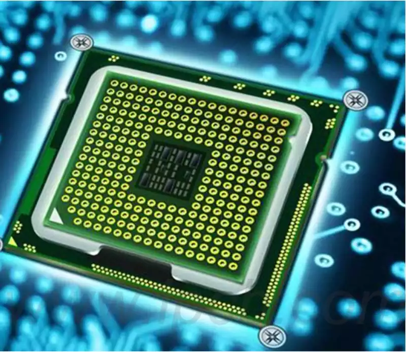
High-frequency pcb board why require low dielectric constant material
When the dielectric constant is large, the ability to store electrical energy is large, and the speed of transmission of electrical signals in the circuit becomes lower. The direction of the current through the electrical signal on the pcb board is usually alternating positive and negative changes,equivalent to the substrate is constantly charging, discharging process, in the interchange, the electric capacity will affect the transmission speed,and this effect,in the high-speed transmission of the device appears to be more important,epsilon low indicates that the storage capacity of the small,charging and discharging process will be fast, so as to make the transmission speed is also fast.Therefore, in the transmission of high-frequency pcb substrate,low dielectric constant is required.
Dielectric loss Df: dielectric material under the action of alternating electric field, due to the heat and the consumption of energy called dielectric loss, usually expressed in terms of the dielectric loss factor tan δ. ε and tan δ is directly proportional to the high-frequency circuits also require ε is low, the dielectric loss of tan δ is small, so that the energy loss is also small.
The basic requirements of high-frequency pcb board
- As a result of high-frequency signal transmission, the requirements of the finished printed circuit board wire characteristic impedance is strict, the line width of the board is usually required to ± 0.02mm (the most stringent is ± 0.015mm). Therefore, the etching process needs to be strictly controlled, optical imaging transfer with the negative needs to be based on line width, copper foil thickness and process compensation.
- This type of printed circuit board is not the transmission of current, but high-frequency electrical pulse signals, pits, notches, pinholes and other defects on the wire will affect the transmission, any such small defects are not allowed. Sometimes, solder resist thickness will also be strictly controlled, line solder resist too thick, too thin a few microns will be judged unqualified.
- Thermal shock 288 ℃, 10 seconds, 1 ~ 3 times, without hole wall separation. For PTFE board, to solve the wettability of the hole, to the chemical sinking of copper holes without cavities, plating in the hole of the copper layer to withstand thermal shock, which is one of the difficulties in making a good Teflon orifice plate.
- Warpage: usually require the finished board 0.5 ~ 0.7%.
With the rapid development of electronic technology, high-frequency PCB boards, as an indispensable component in electronic equipment, have increasingly stringent performance requirements. The dielectric constant DK value, as an important index to measure the electrical performance of PCB boards, and its low-value characteristics are particularly important in high-frequency circuit transmission. Through accurate testing and simulation, we can obtain the exact value of dielectric constant DK, so as to select the appropriate PCB board to meet the operating requirements of electronic equipment.