In recent years, the widespread adoption of smart wearable devices has significantly transformed people’s lifestyles and health management. From smartwatches and fitness trackers to smart glasses and medical devices, wearables have become an integral part of our daily lives. These devices are getting smaller while becoming increasingly more powerful. Behind this transformation lies the innovation in Ultra Thin PCBs (Printed Circuit Boards) and custom-shaped board designs. This article delves into how Ultra Thin PCBs and custom-shaped boards are driving the development of wearable technology and how these advancements are addressing future market challenges.
1.Ultra Thin PCB Design: Small Size, Big Functionality
As wearable devices evolve toward more lightweight designs, Ultra Thin PCB technology has become a core element in modern product design. Traditional PCBs often require significant space to accommodate various electronic components, while Ultra Thin PCBs use advanced manufacturing techniques to reduce the thickness of the circuit board to a minimum, allowing for more compact device designs.
Advantages of Ultra Thin PCBs
Space-saving: Ultra Thin PCBs can house more electronic components within a limited space, reducing the overall size of the wearable device and enhancing the user’s comfort while wearing it.
Lightweight: A thinner PCB not only reduces the overall weight of the device but also increases portability, making the wearable device more comfortable for the user.
Improved Signal Transmission: Ultra Thin designs typically use high-precision manufacturing techniques, reducing the distance between circuits, which minimizes signal loss and improves the efficiency and stability of the device.
Challenges of Ultra Thin PCBs
However, Ultra Thin design comes with its own set of challenges. First, the circuit board’s structure needs to maintain high strength and stability while being thin, ensuring it doesn’t deform or get damaged over prolonged use. Secondly, as the integration of electronic components increases, the thermal management requirements of Ultra Thin PCBs become even more demanding. Thus, effectively distributing space and managing heat dissipation on such a thin circuit board have become critical design challenges.
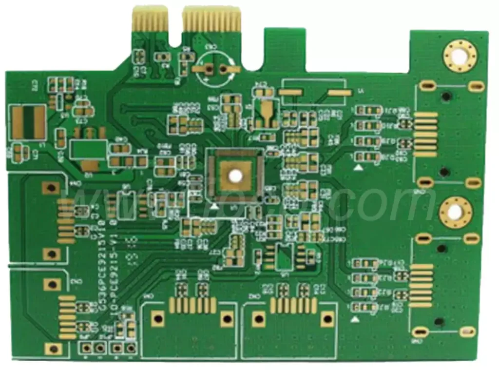
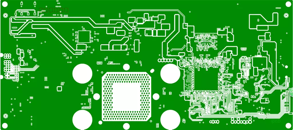
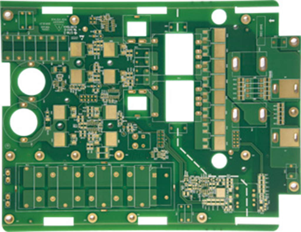
2.Custom-Shaped Board Design: Breaking Tradition and Meeting Personalized Needs
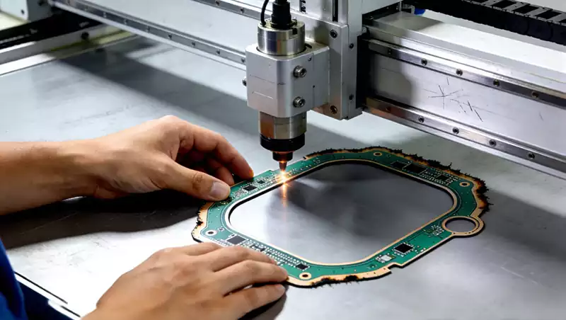
In addition to Ultra Thin designs, custom-shaped board technology has become a crucial innovation in wearable device design in recent years. A custom-shaped PCB refers to a circuit board that is specifically tailored to fit the unique shape and functional requirements of a device. This design approach can greatly enhance the product’s unique appearance while simultaneously fulfilling functional and structural needs.
Applications of Custom-Shaped Boards
Smartwatches and Wristbands: As one of the most representative wearable devices, smartwatches often have round or curved dials that require custom-shaped PCBs to accommodate their special form factor. Custom-shaped boards help maximize the use of limited space while ensuring the stability and reliability of the device’s internal circuits.
Smart Glasses: In smart glasses design, the PCB board needs to fit into very narrow spaces and integrate closely with other components. Custom-shaped boards are essential in achieving this level of precision and compactness.
Wearable Medical Devices: With the growing demand for wearable medical devices, custom-shaped boards are increasingly used in products such as ECG monitors and blood glucose meters, where the complex shapes of the devices need to be matched while maintaining wearability and accuracy.
Advantages and Challenges of Custom-Shaped Boards
While custom-shaped boards provide unique form factors and personalized designs, they also present manufacturing challenges. Due to their irregular shapes, the precision requirements in production are higher, and the complexity of the manufacturing process increases. Furthermore, custom-shaped boards often require more intricate electrical connections and assembly, setting higher standards for production equipment and techniques.
3.The Synergy of Ultra Thin PCBs and Custom-Shaped Boards: Creating Smarter Wearables
Both Ultra Thin PCBs and custom-shaped boards have their own distinct advantages, but when combined, their benefits are unparalleled. In many modern wearable devices, these two design approaches are often inseparable. For example, the round dial of a smartwatch not only requires Ultra Thin PCB technology but also needs custom-shaped boards to adapt to its curved and compact internal space. Through this synergy, device designs can meet the needs of highly integrated electronic components while maintaining a lightweight, stylish appearance.
Looking Ahead: The Future Development of Ultra Thin and Custom-Shaped Technologies
With ongoing advancements in materials science and manufacturing processes, the potential for Ultra Thin PCBs and custom-shaped boards will continue to grow. For instance, the development of flexible PCBs (FPC) enables even thinner and more flexible circuit boards, opening up new possibilities for wearable device design. Furthermore, with the continued maturation of technologies such as 5G, AI, and the Internet of Things (IoT), future wearable devices will become more intelligent, requiring even more precise and efficient circuit board designs.
The application of Ultra Thin PCBs and custom-shaped boards in smart wearable devices has become a key driver of industry progress. As consumer demand for wearables grows more diverse and personalized, the combination of Ultra Thin designs and custom-shaped boards will become the mainstream trend in wearable device design. Despite the challenges in manufacturing, these technologies, driven by continuous development and innovation, will bring even more possibilities to future smart wearables, fulfilling users’ expectations for lightweight, comfortable, and intelligent devices.