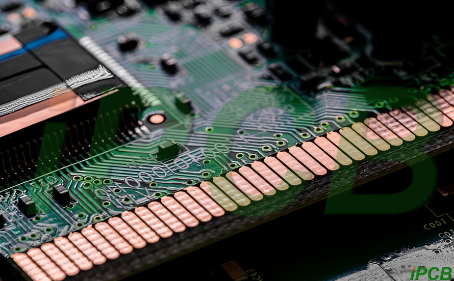
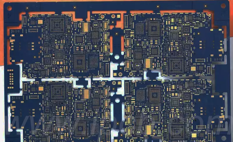
Wafer Level Packaging (WLP) is an advanced packaging technology that refers to the direct encapsulation of chips onto wafers to form a complete whole (similar to a microcircuit), and the final product is a chip module containing chips, pins and connecting wires. There are three main technology routes for wafer-level packaging: BGA (Ball Grid Array), CSP (Chip-Scale Package) and WLCSP (Lead-free Wafer-Level Package). Packaging on wafers can directly reduce production costs, improve product reliability and meet the production needs of compact and miniaturized mobile devices.
Wafer-level packaging process flow is as follows:
- Coating the first layer of polymer film to strengthen the chip passivation layer, play the role of stress buffer. Polymer types include photosensitive polyimide (PI), benzocyclobutene (BCB), and polybenzoxazole (PBO).
- Rewiring layer (RDL) is the location of the chip’s aluminum/copper solder area re-layout, so that the new solder area to meet the requirements of the minimum pitch of the solder ball, and so that the new solder area in accordance with the array row. The photoresist is used as a template for selective plating to plan the line pattern of the RDL, and finally wet etching removes the photoresist and sputter layer.
- A second polymer film is coated to flatten the wafer surface and protect the RDL layer. The new solder area is photolithographed on the second polymer film.
- The Under Bump Metal Layer (UBM) is fabricated using the same process as the RDL.
- Ball Placement. The solder paste and solder ball are accurately positioned through the mask plate, the solder ball is placed on the UBM and put into the reflow oven, the solder is melted by reflow to form a good infiltration bond with the UBM to achieve good soldering results.
Wafer Level Packaging VS Traditional Packaging
In traditional wafer packaging, finished wafers are cut into individual chips and then bonded for packaging. Unlike the traditional packaging process, wafer level packaging is to encapsulate the chip when the chip is still on the wafer, the protective layer can be glued to the top or bottom of the wafer, and then connected to the circuit, and then cut the wafer into individual chips.

Compared with traditional packaging, wafer-level packaging has the following advantages:
Small package size
Since there are no leads, bonding and plastic processes, the package does not need to be extended outside the chip, making the package size of WLP almost equal to the chip size.
High transfer speed
Compared with traditional metal-lead products, WLPs generally have shorter connection lines and will perform better under high performance requirements such as high frequency.
High Density Connections
WLP can utilize array connection, the connection between the chip and the board is not limited to the perimeter of the chip, increasing the connection density per unit area.
Short Production Cycle
The whole process of WLP from chip manufacturing to packaging to finished product, the intermediate links are greatly reduced, the production efficiency is high, and the cycle time is much shorter.
Low process cost
WLP is completed at the wafer level packaging test, to achieve the goal of cost minimization in a batch production mode. the cost of WLP depends on the number of qualified chips on each wafer, the chip design size reduction and the trend of increasing the size of the wafer so that the cost of a single device package to reduce the cost of the corresponding. WLP can make full use of wafer fabrication equipment, the low cost of production facilities.
Low cost analysis of wafer-level packaging
Low cost of basic materials
The base material for wafer-level packaging is silicon substrate, which is relatively low cost in case of large quantity. As new process technology continues to introduce new, wafer-level packaging base material costs will continue to decrease.
Simple process
The production process of wafer-level packaging is simpler than traditional packaging, and there is no need to add additional packaging components outside the chip, which reduces the cycle time of product testing, packaging and verification, and thus improves production efficiency.
High Production Efficiency
Wafer-level packaging is highly productive, and at the same time, it also reduces many intermediate links, such as chip processing, pin making, etc.. This reduces problems such as material waste that may occur during the production process, thus reducing costs.
High flexibility
The production method of wafer-level packaging allows for rapid changes and updates of chips and pins, which simplifies the production and design process, thus greatly improving the flexibility and resilience of the production process.
With its unique advantages, wafer-level packaging technology is becoming the new favorite in the packaging field. It meets the market demand for compact and miniaturized electronic products and is leading the new development of the packaging industry with its high efficiency and low cost.


