As an integral part of the electronics manufacturing industry, wave soldering has a direct impact on the performance and reliability of electronic products in terms of soldering quality. Optimising the wave soldering process means striving for excellence in every detail to ensure that every solder joint is the best it can be.
Wave soldering typically consists of three basic sub-processes: flux application, preheating and soldering. Optimising the wave soldering process means optimising these three sub-processes. Among these sub-processes, the most critical elements are the following:
1) The importance of dwell time optimisation and reproducibility in the soldering process
The optimisation of the dwell time and its reproducibility is crucial for the welding process. To achieve this, efforts should be made to obtain instantaneous data on the PCB as it exits from the brazing wave and to provide direct measurements of the immersion height. The specific operation procedures include: first, ensuring that the PCB remains parallel to the wavefront; second, measuring the PCB’s residence time in real time; third, measuring the PCB’s immersion depth in real time; and finally, evaluating the soldering quality of the PCBA to derive the actual defect rate (ppm). Of these, the first three operations need to be performed twice per shift (8 hours), while the last one should be completed at the end of each shift. Prior to PCB soldering, once the measurement results are found to show non-parallelism or changes in dwell time or immersion depth, the wave soldering machine should be adjusted immediately to ensure that the expected interaction between the board and the wave is achieved, so as to realise the reproducibility of the PCB soldering quality.
2) Influence of immersion depth on weld quality
Changes in immersion depth directly affect the contact length and residence time, so it is particularly important to have a direct and accurate measurement of the immersion depth. The crest height is determined by the pump speed and decreases with the consumption of brazing material in the brazing tank. The actual immersion depth of the PCB is affected by a number of factors, including the height of the brazing bath, how the PCB is held in the conveyor fingers, the angle of the conveyor, and whether or not brackets are used.
Controlling the immersion depth to keep it constant is only part of the problem, it is more important to determine at which immersion height the PCB can be soldered with the best quality. To summarise, the following conclusions can be drawn: the defect rate varies significantly with dwell time; controlling the immersion depth is critical because a change in the immersion depth implies a change in the contact length, which results in an uncontrollable dwell time; the optimisation of the interaction between the PCB and the brazing wave has significant benefits, and the different types of PCB need to be evaluated on a case-by-case basis when deciding on the wave soldering process. Using the same parameters for all PCBs is unlikely to all achieve optimum soldering results; optimisation is a dynamic adjustment process based on statistical data on actual defects on the PCB, and recording only machine settings or static data on the PCB and wave will not achieve the desired results.
3) The role of flux and coating
Flux is used to increase the level of surface energy of the soldered base metal, thereby improving the wettability of the surface to be soldered. The flux used for soldering of electronic products has a wide range of activity, ranging from corrosive organic acids to weak organic acids. The corrosiveness of rosin-based fluxes depends on the type and content of halides. Residues of some rosin-based materials can remain on the PCB after soldering because the active agent is sealed by the rosin resin envelope and shows no activity to the outside world. The ratio of rosin to active agent determines how well the active agent is sealed by the rosin encapsulation. Currently, most of the flux used in no-clean wave soldering are weak organic acid formulations.
The flux coating must be uniform and of controlled thickness, and needs to penetrate the hole and spread to the pins.
4) the role of preheating in the wave soldering process
In the wave soldering process to add preheating process has multiple roles. Firstly, before the flux works, the active agent in it needs to be chemically broken down, and these active chemical components then interact with the oxide on the surface of the base metal to remove the oxide. Therefore, the flux must be preheated to the activation temperature to initiate this reaction. Secondly, preheating accelerates the evaporation of volatiles, thereby eliminating potential problems that can occur in wave soldering. These volatiles come primarily from the flux, but can also originate from the PCB manufacturing, storage and distribution processes. The presence of volatiles on the wave crest may trigger braze ball spatter. Again, preheating gradually increases the temperature of the soldered component, thereby minimising the harmful thermal shock to the PCB and installed components during the wave soldering process, relieving thermal stresses, and thus reducing warping and distortion of the printed board. Finally, the preheating treatment can increase the pre-soldering temperature of the PCB assembly, so that the PCB can be heated to the wetting temperature of the soldered part more quickly when it comes into contact with the brazing wave, thus speeding up the clamping speed of the conveyor belt. This not only improves production efficiency, but also has the advantages of attenuating the excessive metallurgical phenomenon that occurs between the filler brazing material and the base metal in the solder seam, and suppressing the thermal deformation of PCBs, components, plastic parts and so on.
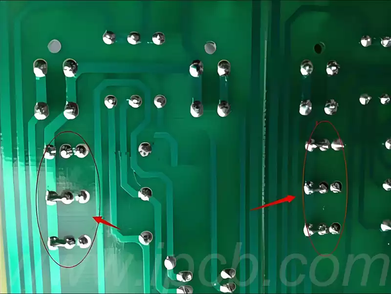
Some suggestions for wave soldering process:
1.A lot of defects in the wave soldering clock with the PCB design, must consider the DFM
2.A lot of defects and PCB. SMD processing components quality, in order to avoid the impact of counterfeit and shoddy components on the quality. Should choose qualified suppliers, controlled logistics. Storage conditions.
3.Many defects stem from the flux activity is not enough. Good flux can withstand high temperatures,prevent bridging, and improve through-hole tin permeability.
4.Wave soldering temperature should be set as low as possible to prevent component overheating.Material damage. Especially to control the mixing process in the second melting tin.
5.Low solder temperature can reduce solder oxidation, reduce slag, reduce the molten solder on the solder tank and impeller erosion. Limit the generation of FeSn2 crystals.
6.Excellent process control can reduce the level of defects. Comprehensive adjustment of process parameters should be carried out, and must control the temperature profile.
7.Pay attention to the maintenance of solder in the tin furnace, and strengthen the routine maintenance of equipment.
Optimisation of the wave soldering process is the key to improving the manufacturing quality of electronic products. By optimising the wave soldering process, it can effectively reduce soldering defects and improve production efficiency.
