In the circuit board design process, PCB layers, or printed circuit board layers, refer to the division and stacking of different functional areas during the circuit board manufacturing process.
Layers that are used more often in PCB design:
mechanical mechanical layer
Keepout layer Disable wiring layer
Signal layer Signal layer
Internal plane layer Internal power/ground layer
top overlay top screen printing layer
top overlay bottom overlay
top paste top flux layer
Bottom paste Bottom flux layer
top solder top solder resist
bottom solder Bottom solder
drill guide Drill guide
drill drawing
multilayer multilayer
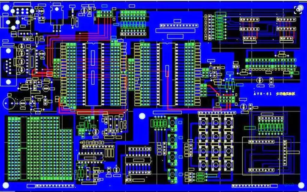
PCB layers are mainly composed of several sub-layers with different functions. The top layer is primarily used to house components and serves as a reference layer for multilayer board wiring comparisons. The middle layer, on the other hand, has up to 30 layers and is used to lay out signal lines in a multilayer board. The bottom layer, also known as the soldering layer, is primarily used for wiring and soldering operations, and sometimes components can be placed on the top screen layer.
PCB layers also include other key sub-layers. Solder mask layer, consisting of the top and bottom solder mask layers, protects the pads and via data. The Solder Paste Layer, consisting of the top and bottom layers of solder paste, is the exposed portion of the surface mount pads and the area where solder paste is applied for soldering. The silkscreen layer, on the other hand, is used to identify component outlines, labels, labeled values, etc. for easy soldering and inspection.
The Mechanical Layer is another important part with up to 16 machining layers. It defines the entire profile of the PCB board and is typically used to place information indicative of the manufacturing and assembly methods, such as form factors, dimensional markings, datasheets, and so on. These layers play a key role in the manufacturing and assembly process of the board.
Also, the in-plane layers are unique to multilayer boards. They are usually connected to the power and ground lines, forming the power and ground layers. Although these layers are not usually used for wiring, they play an important role in the electrical connections of a circuit board.
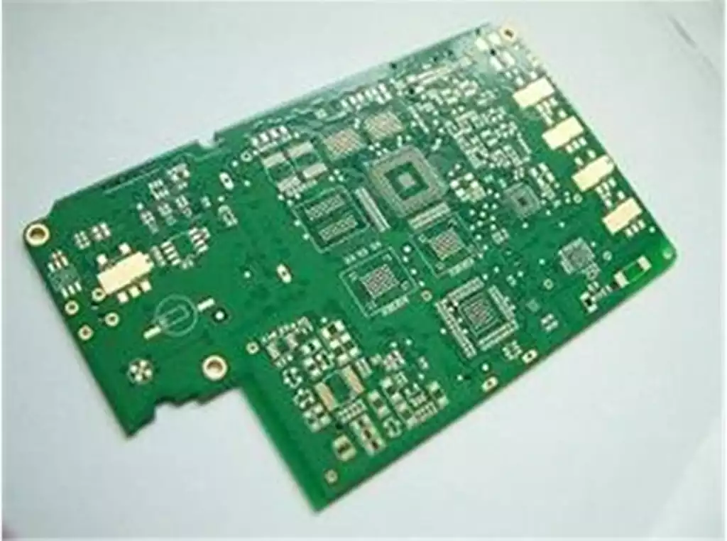
Paste mask layer (flux layer, SMD patch layer):
It is similar to the role of the soldermask layer, the difference is in the machine soldering corresponding to the surface of the paste components of the pad.Altium Designer provides Top Paste (Top Paste) and Bottom Paste (Bottom Paste) two flux layer. Mainly for SMD components on the PCB. In the SMD components on the circuit board before the SMD pads must be coated with solder paste in each first, in the coating of tin with the stencil must need this Paste Mask file, film film can be processed out of the Paste Mask layer of the Gerber output the most important point to be clear, that is, the layer is mainly for the SMD components, at the same time the layer with the above introduction of the Solder Mask for a comparison, to clarify the different roles of the two, because the two film from the film film map is very similar to see the film map.
Distinction between Solder Resist Layer and Flux Layer
Solder mask: solder mask, is the part of the board to be on the green oil; because it is a negative output, there is no solder mask area to be on the green oil, so in fact there is a part of the actual effect of the solder mask and not on the green oil.
Soldering layer: paste mask, is the machine to be used when the patch, is corresponding to all the patch components of the pad, the size of the toplayer/bottomlayer layer is the same, is used to open the stencil leakage of tin with.
PCB layers play a pivotal role in circuit board design. By gaining an in-depth understanding of the function and purpose of each layer, designers can build circuit boards more accurately and ensure the stability and reliability of their circuits.
