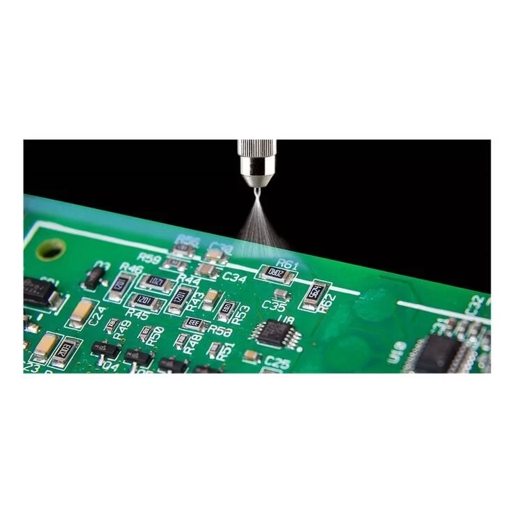
Gold plated PCB boards are made by electroplating a layer of gold on the pads of the PCB circuit board, which consist of hard gold. The process involves dissolving nickel and gold in a chemical solution and then immersing the board in a plating bath, which is energized to form a nickel-gold coating on the copper foil of the board.
Gold plating is a type of PCB surface treatment also known as nickel-gold plating. In the PCB manufacturing process, gold plating is realized by depositing a layer of gold on the nickel barrier layer by electroplating. Gold plating can be divided into “hard gold plating” and “soft gold plating”.
The role of gold plating:
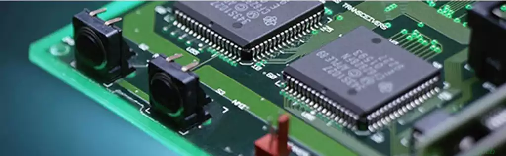
The two key properties of gold plating are wear resistance and corrosion resistance. Components that require gold plating include parts with sockets and gold fingers, as well as areas in contact with conductive rubber. Boards that operate in highly corrosive environments should also use gold-plated boards. Gold plating prevents oxidation and protects the nickel and copper underlayment. The abrasion resistance of gold makes it highly reliable.
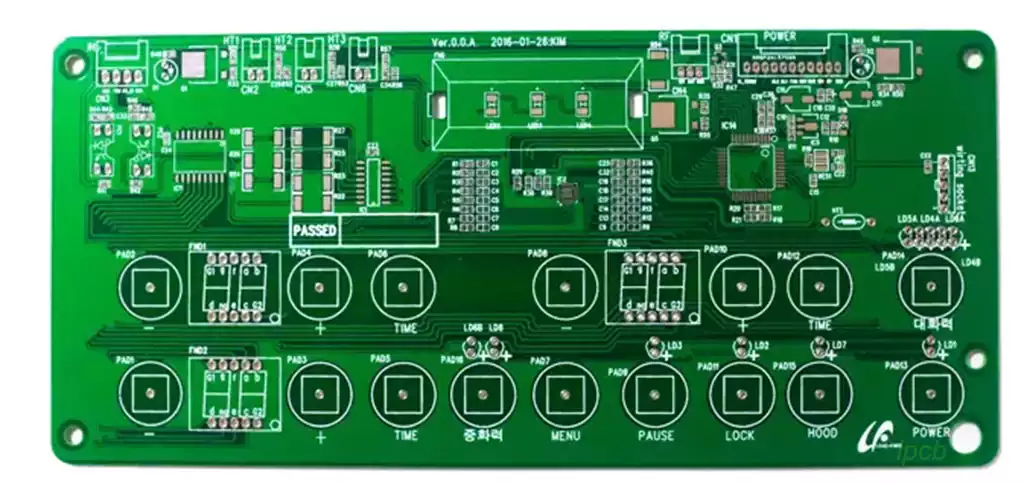
Advantages of gold-plated PCB boards include high conductivity, good oxidation resistance, and long service life. Their dense and relatively wear-resistant coating is commonly used for soldering and socket applications. The gold plating process is widely used for circuit board components such as pads, gold fingers, connector shrapnel and other locations. Most of our commonly used handheld circuit boards are gold plated.
Gold plating has low contact resistance, good electrical conductivity, easy soldering, strong corrosion resistance, and some abrasion resistance (refers to hard gold). It is widely used in precision instruments, printed circuit boards, integrated circuits, tube housings, electrical contacts and other fields.
The difference between soft gold and hard gold:
In PCB plating process, hard gold plating is also known as plating alloy. It combines with other elements to form an alloy, making it harder, while soft gold plating is pure gold.
Application of gold plating in PCB manufacturing: Hard gold plating is used in areas such as gold fingers and keyboards where friction is required. Soft gold is typically used for aluminum or gold wiring on COBs (chips on boards).
Difference between PCB gold plating and electroplating:
Process Principle: PCB gold deposition is the process of depositing metal ions on the surface of a circuit board. In this process, the board is immersed in a solution containing gold salts and a reducing agent, and the gold ions are reduced to metal and deposited on the surface of the board. Gold plating is a process in which a circuit board is immersed in a solution containing gold salts and then energized to deposit gold ions on the surface of the board.
Metal thickness: PCB gold deposition and gold plating have different metal thicknesses. Gold deposition can form a relatively thick metal layer, usually up to 2-5 microns. Gold plating metal layer is relatively thin, usually only about 0.5-1.5 microns.
Metal color: The metal color of PCB gold deposition and gold plating is also different. The metal color of immersion gold is golden yellow, while the metal color of gold plating is light yellow.
Surface flatness: The surface flatness of PCB Immersion Gold and Gold Plating is also different. Immersion gold has a relatively flat surface, which maintains high-quality soldering and contact effects. Gold plating has a relatively rough surface and is prone to soldering and contact problems.
Cost: The cost of PCB gold plating and electroplating also differ. The cost of gold plating is relatively high because it requires more chemicals and longer processing time. The cost of gold plating is relatively low because it has short processing time and simple operation.
PCB gold plating process flow:
Gold plating is widely used in precision instruments, printed circuit boards, integrated circuits, tube casings, electrical contacts and other fields because of its low contact resistance, good electrical conductivity, easy soldering, strong corrosion resistance, and a certain degree of abrasion resistance (refers to hard gold). Its process includes the following steps:
Surface treatment: clean the surface of PCB, remove oil, burrs, oxide layer and other impurities.
Plating: Place the PCB into the plating tank and add plating solution. The plating solution contains a reducing agent, which can reduce the gold atoms on the PCB surface to metal ions and deposit them on the PCB surface.
Rinsing: After plating is completed, the PCB surface needs to be cleaned with water to remove the residual plating solution and metal deposits.
Drying: The PCB is placed in a drying oven and heated to remove moisture.
Adhesive Coating: A layer of conductive adhesive is applied to the circuit board surface to ensure good contact between the PCB and other equipment.
Recycling: Remove the PCB from the tape and place it into a recycling bin for subsequent disposal or reuse.
Gold plated PCB boards can play a protective role. The gold-plated layer can prevent the board from oxidation, corrosion and other effects, thus prolonging the service life of the board. The metal itself has good conductivity, which can improve the conductivity of the PCB and reduce the line impedance.