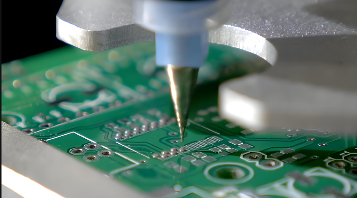
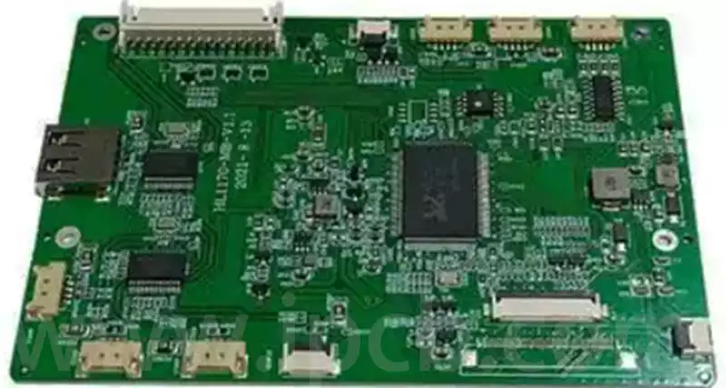
Wafer testing is divided into two main categories: wafer testing (CP testing) and finished product testing (FT testing). Wafer testing is a moderate test of the capacitance and circuit function on each wafer after wafer fabrication is completed to ensure that its circuits are functioning properly before it is sent to the packaging plant for packaging. Finished product testing, on the other hand, is the final test after wafer packaging is completed. The test nodes, test plans and procedures during the wafer packaging process may vary depending on the type of wafer. Therefore, in order to meet customers’ needs for end-product quality rate improvement and cost control, we prefer to provide customized services.
The wafer BA17807T testing industry has always been regarded as a part of wafer seal testing. However, looking at the overall situation of the domestic wafer industry, the traditional integrated package testing enterprises can no longer meet the current demand. The testing business of these companies is often only a supplement to the packaging business, and their core business mainly involves packaging and testing, which cannot fully serve customers or respond to the needs of external users.
With the rapid development of the wafer design industry, some companies have wafer design capabilities but lack wafer testing capabilities. As a result, after designing a large number of wafer types, they remain at the design stage and are unable to perform package testing, let alone talk about production and marketing. This means that there is a large unmet demand for wafer testing, and the industry has a growing need for wafer testing businesses. Wafer testing companies can adjust wafer design concepts in the testing process according to customer needs, and even provide customized testing services to meet the stringent requirements for wafer functionality, performance and quality.

However, the wafer testing industry is both technology-intensive and capital-intensive, which is closely related to the technological and capital strength of companies. In addition, mainland Chinese companies are now showing strong growth momentum due to their late entry into the wafer testing market. According to TrendForce’s 2021 report, six of the top ten manufacturers in the global sealed test market are from Taiwan, accounting for 54.8% of the total market share; three of them are from mainland China, accounting for 27%; only Ankao is from the US, with market shares of 17% and 9% respectively. Nevertheless, there are not many companies in China that can engage in the wafer testing business, but the market still has a lot of room for development.
Among them, GTC is a transistor company that can engage in independent wafer testing business. GTC has introduced advanced testing equipment from the Netherlands, Japan, the United States, Hong Kong and other countries and regions, and formed a scientific and technological team with rich experience in the semiconductor industry and professional equipment configuration. At present, wafer testing has shown a gradual trend towards high-end. It is difficult for traditional closed testing companies to have enough money and energy to cope with the industry changes, but they may pay attention to this market.
Regarding aging test in wafer testing, it is an electrical stress test method that detects electrical failures in gas pedal components by applying voltage and high temperature. The aging process simulates the entire life of the wafer, as the electrical excitation applied during aging reflects the worst-case scenario of wafer operation. Depending on the aging time, the reliability of the data obtained may relate to the early life of the device or the level of wear and tear. Aging tests can be used as a device reliability test or as a production window to detect early device failures. Commonly used wafer aging test equipment determines wafer qualification by testing wafer data obtained by working with sockets and external circuit boards.
Transistor failures can be categorized into three types: early failures, random failures, and wear-out failures. Early failures occur during the initial stages of equipment operation and diminish over time; random failures occur over a longer period of time and at a constant rate; and wear-out occurs at the end of a component’s shelf life. To ensure product reliability, reducing early failures is critical. Aging tests allow for the detection of potential defects in the transistor that become apparent when the device is subjected to voltage stress and heating and begins to operate. Most early failures are caused by the use of defective manufacturing data and errors encountered during the production phase. Only wafer assemblies that undergo aging tests and show a low rate of early failures are released to the market.


