What is osp? OSP is a RoHS compliant process for the surface treatment of copper foil on printed circuit boards. It is short for Organic Solderability Preservatives, which translates to Organic Solderability Film, also known as Copper Protectant, and also known as Preflux in English. method to grow a layer of organic film. This film has anti-oxidation, thermal shock, moisture resistance, to protect the copper surface in the normal environment will not continue to rust (oxidation or sulfidation, etc.); but in the subsequent welding high temperature, such a protective film and must be easy to be flux quickly removed, so that the exposed clean copper surface to be in a very short period of time and the molten solder immediately combined with a solid solder joints.
Purpose of OSP surface treatment process
The main purpose of OSP surface treatment process is to form a layer of protection against oxidation on the PCB board to improve product reliability and stability. At the same time, the OSP surface treatment process can also reduce the impact on subsequent processes, such as drilling and assembly.
Process flow of OSP surface treatment process:
(1) Cleaning: first of all, the PCB board is cleaned to remove oil, dust and other impurities.
(2) Pre-treatment: Pre-treatment of PCB boards, including chemical cleaning, oxidation removal, etc..
(3) OSP solution treatment: PCB board immersed in OSP solution, through the control of the solution temperature, concentration and time, so that the PCB board surface to form a layer of protective layer to prevent oxidation.
(4) Drying: Remove the PCB from the OSP solution and dry it to remove excess water and solvent.
(5) Inspection: PCB boards are inspected to ensure that their surface quality and performance meet the requirements.
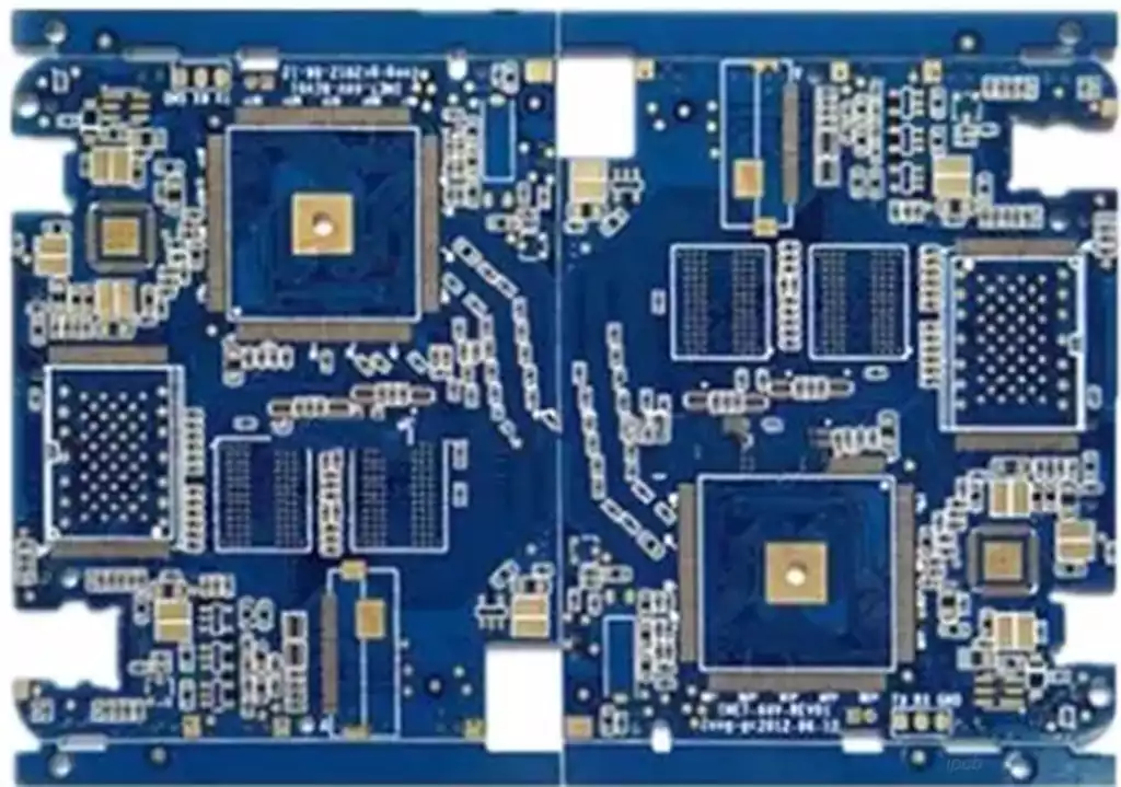
OSP surface treatment process requirements
(1) cleaning requirements: cleaning is the first step in the OSP surface treatment process, the cleaning effect directly affects the quality and performance of subsequent processes. Therefore, the cleaning agent used in the cleaning process should have a good ability to remove oil and dust and other impurities, and should also have a low-toxicity, environmentally friendly features.
(2) pretreatment requirements: pretreatment is to remove the oxide layer and other impurities on the surface of the PCB board, in order to improve the effectiveness of the OSP surface treatment process. Therefore, the pretreatment process should be used in the chemical cleaning agents and oxidation removal agents, etc., in order to achieve the desired results.
(3) OSP solution treatment requirements: OSP solution treatment is the core link of the OSP surface treatment process, and its treatment effect directly affects the surface quality and performance of the PCB board. Therefore, the requirements of the OSP solution temperature, concentration and time and other parameters should be strictly controlled to ensure that the surface of the PCB board to form a uniform, dense protective layer.
(4) Drying requirements: drying is to remove excess water and solvents on the surface of the PCB substrate to ensure its surface quality and performance. Therefore, the drying process should be used in the appropriate drying equipment and methods to ensure that the moisture and solvent content on the surface of the PCB board to meet the required standards.
(5) Inspection requirements: inspection is to ensure that the surface quality of the PCB board and performance in line with the requirements of the important links. Therefore, the inspection staff should have good inspection skills and equipment, but also to develop strict inspection standards and methods to ensure product quality and performance.
OSP process advantages
(1), cost-effective. OSP is an organic material, its performance is good, the price is cheaper than the spray metal tin process.
(2), good chemical performance. OSP has very good chemical performance, can be very good to ensure that the inner layer of copper foil will not be oxidized.
(3), good thermal shock and moisture resistance, in the production environment can prevent copper oxidation, sulfidation.
(4) Good operability. Normal state to ensure that the inner layer of copper foil will not be oxidized, and when welding due to the heating makes the film layer volatile, easy to solder the copper and components welded.
Disadvantages of OSP process
Low recognition. OSP boards have been used because of the transparent colorless and normal boards are basically the same, it is difficult to directly identify the need for special marking.
②, with insulating properties, OSP insulation is not conductive, will affect the electrical testing of PCB boards, need to remove the surface film layer to normal testing.
③, poor corrosion resistance, susceptible to acidic substances and temperature, exposure to air for more than 24 hours, it is necessary to carry out the second OSP process as appropriate.
⑤, affecting other SMT processes and defects adjustment. For example, the board can not be printed poorly IPA cleaning, will damage the OSP film layer; Cu of the pad and the solder between the Sn of the pad is not IMC isolation, in the lead-free technology, high Sn content of Sn in the solder joints in the SnCu grows very quickly, affecting the reliability of the solder joints.
(vi) Poor stability of the film layer. For example, the thickness of the film layer is difficult to stabilize; process formulations of a variety of performance varies; the film layer is easy to scratch; many high-temperature soldering process of the OSP is prone to discoloration, cracks, thus affecting the solderability and reliability; operation and storage and transportation requirements, etc..
