What is PCB Contamination? In the electronic manufacturing process, many failure problems do not stem from design errors or component quality, but from a long-underestimated factor—contamination. Understanding what PCB contamination is involves more than simply determining whether the board is “dirty”; it requires recognizing how various seemingly minor residues can gradually erode the reliability of the circuit during actual operation. These problems often don’t show up immediately during factory testing, but may suddenly appear weeks, months, or even years later, posing a continuous risk to system stability and brand reputation.
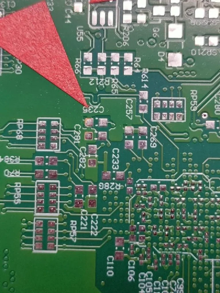
From an engineering perspective, PCB contamination refers to foreign substances present on the board surface, pads, conductors, or vias that are not intended as part of the design during the manufacturing, assembly, or use of the circuit board. These substances may originate from chemical processes, assembly steps, human contact, or environmental exposure, and include ionic residues, organic flux residues, grease, dust, moisture, and corrosive gases. They may not immediately cause short circuits or open circuits, but under the combined effects of electric fields, humidity, and temperature, they gradually alter electrical behavior.
The danger of PCB contamination lies in its “latent” nature. Unlike obvious soldering defects, broken wires, or component failures, contamination often shows no abnormalities during board functional testing; the circuit appears completely normal. However, once the circuit operates under high humidity, high voltage, or high frequency conditions, the ions in the contaminants begin to migrate, forming weak conductive paths between conductors, leading to leakage current, increased signal noise, and even electrochemical corrosion. These failures typically manifest as intermittent problems, making them difficult to reproduce and extremely difficult to quickly pinpoint the root cause.
In analog circuits and low-frequency systems, slight contamination may not be significant; however, in high-speed digital, high-frequency radio frequency, or high-density designs, the impact of contamination is amplified. For example, on high-speed signal lines with strict impedance control, residual ions and organic matter can alter the local dielectric environment, causing signal propagation characteristics to shift; in radio frequency applications, contamination increases dielectric loss and parasitic effects, directly affecting system sensitivity and signal-to-noise ratio. This is why, as electronic products become higher in frequency and smaller in size, PCB contamination has evolved from a “manufacturing detail” to a “system-level risk.”
It is important to note that PCB contamination is not the same as “not being cleaned properly.” Many circuit boards that meet process specifications and pass conventional microscopic inspection or electrical performance tests still harbor potential problems under specific conditions. This is why more and more companies in the industry are introducing ionic contamination testing, surface insulation resistance (SIR) testing, and accelerated environmental aging testing—because contamination issues need to be evaluated through long-term behavior, not just the current state.
From a quality management perspective, understanding what PCB contamination is is also a crucial basis for defining manufacturing responsibilities. Contamination can occur at the board manufacturer, during surface mounting, component insertion, rework, or final assembly, or even from the end-use environment. Only by clearly defining the type, source, and mechanism of contamination can effective prevention and control strategies be established throughout the entire supply chain, rather than engaging in repeated disputes after problems arise.
Therefore, PCB contamination is by no means a simple matter of “cleanliness,” but a comprehensive issue involving materials, chemistry, processes, electrical performance, and long-term reliability. A truly mature electronic manufacturing system must consider contamination control as a fundamental capability equally important to circuit design, lamination structure, and soldering quality.
Main Types and Formation Mechanisms of PCB Contamination
The first step in understanding what PCB contamination is is to clarify its main types and formation mechanisms, because different types of contamination not only affect circuit performance differently, but also require different prevention and detection methods. In actual manufacturing and assembly processes, contaminants can be broadly divided into four categories: ionic contamination, organic residues, particulate contamination, and environmental chemical corrosion, each of which poses a potential threat to system reliability.
First is ionic contamination, which usually originates from flux residues, incomplete washing, or volatile solvents in the air. Ionic contamination on PCBs manifests as mobile salts and metal ions. These ions easily form micro-conductive paths in high-humidity environments, leading to leakage current, dielectric breakdown, or intermittent short circuits. Especially in high-density wiring and high-impedance control lines, even trace amounts of ions can significantly alter the local electric field distribution, causing distortion of high-speed signals and increased error rates.
Secondly, there are organic residues, including organic components of flux, cleaning agent residues, hand sweat, or lubricants. Although organic materials are generally non-conductive, they can absorb moisture, altering their insulating properties. Furthermore, under high temperatures, they may undergo decomposition or oxidation reactions, generating acidic substances or corrosive byproducts. These contaminants form a thin film on the PCB surface, and over time, this accumulation can cause potential damage to solder joints, copper traces, and metal surfaces, leading to performance degradation in aging or high-humidity environments.
Particulate contamination includes dust, tiny metal fragments, fibers, or particles generated from tooling wear. These contaminants are often visually detectable, but fine particles, especially in micro-pitch, high-density wiring areas, are extremely difficult to remove. Particulate contamination can cause localized electric field distortion, creating a risk of short circuits and even triggering soldering defects. Additionally, they may char during high-temperature reflow soldering, forming carbides, further increasing local conductivity and thus reducing system reliability.
Finally, there is environmental chemical corrosion contamination, primarily stemming from PCBs being exposed to corrosive gases (such as hydrogen sulfide, chlorides, and ammonia) and high-humidity environments during manufacturing, storage, or transportation. The metal surfaces, affected by these gases, form oxide layers or sulfides in microscopic areas, altering the surface impedance of the copper traces and affecting signal transmission characteristics. Over long-term use, this type of contamination can lead to open circuits, intermittent failures, or increased signal noise, especially in high-frequency or high-precision signal lines, where the impact is amplified several times.
The mechanism of contamination formation is a multi-factor coupled process. In PCB production and assembly, every step can potentially generate contamination: printing, lamination, drilling, etching, deburring, cleaning, component placement, reflow soldering, testing, rework, and final packaging and transportation. Environmental factors such as temperature, humidity, air cleanliness, and operating practices directly influence the type and degree of contamination. For example, the same flux, if used under conditions of high humidity or insufficient cleaning, may result in ion residue levels far exceeding normal standards, creating difficult-to-detect hidden hazards.
Therefore, understanding what PCB contamination is involves not only recognizing the contamination itself but, more importantly, grasping its generation mechanisms and modes of action. Only by thoroughly analyzing the sources, types, and formation conditions of contamination can engineers implement effective prevention and control strategies during the design, manufacturing, and testing phases, thereby significantly reducing future risks and improving the reliability and lifespan of the entire system.
The Real Impact of PCB Contamination on Circuit Performance and Long-Term Reliability
After understanding what PCB contamination is, what truly needs attention is how these seemingly trace, invisible contaminants gradually affect circuit performance and ultimately lead to system-level failures. The harm of PCB contamination is not instantaneous, but rather its negative effects are continuously amplified over time through the combined action of time, environment, and electrical stress. This is one of the core reasons why many electronic products pass early testing but frequently fail in field applications.
First, contamination has the most direct impact on electrical insulation performance. The insulation design of PCBs essentially relies on the high surface resistance and stable dielectric properties of the materials. Ionic residues and hygroscopic organic substances significantly reduce surface insulation resistance. When the circuit operates in high-voltage or high-humidity environments, these contaminants provide a path for charge migration, generating weak but persistent leakage currents. Although this leakage current is usually insufficient to trigger an immediate short circuit, it can cause significant deviations in precision analog circuits, high-impedance input stages, or sensor systems, resulting in measurement errors or unstable operating conditions.
Secondly, PCB contamination has a profound impact on signal integrity, especially in high-speed and high-frequency systems. Contaminants adhering to the surface of the traces or the dielectric interface alter the local dielectric environment, causing subtle but uneven changes in impedance. For high-speed digital signals, this impedance discontinuity leads to reflections, jitter, and eye diagram shrinkage; in radio frequency systems, contamination introduces additional losses and parasitic effects, causing signal amplitude reduction and increased phase shift, ultimately affecting the sensitivity and stability of the system. These problems are often difficult to detect through conventional electrical testing but are continuously amplified in complex operating conditions.
Thirdly, contamination is a major cause of electrochemical migration and metal corrosion. Under the combined action of humidity, voltage gradients, and ionic contamination, electrochemical migration occurs between metal conductors, forming metal dendrites. These dendrites initially exist only on a microscopic scale, but over time, they gradually grow and eventually form conductive paths, leading to short circuits or intermittent failures. Unlike mechanical damage, this type of failure is sudden and often manifests as a device suddenly malfunctioning at a certain point in time, yet it is difficult to find a clear cause through visual inspection.
From a long-term reliability perspective, PCB contamination also accelerates the aging process of materials and solder joints. Organic residues may undergo chemical decomposition in high-temperature environments, generating acidic substances that corrode the solder pads and solder joint surfaces, reducing metal bonding strength. With repeated thermal cycling and mechanical stress, the risk of solder joint fatigue and poor contact increases significantly, and these problems are more likely to reappear after rework, posing continuous challenges to maintenance and quality control.
It is important to emphasize that the impact of contamination is highly environment-dependent. In a dry, low-pressure laboratory environment, contamination problems may remain latent for a long time; however, once the product is put into a humid, high-temperature, or high-voltage actual application environment, the probability of failure increases significantly. This is why some products pass all tests in the laboratory but frequently receive complaints after actual delivery. Understanding what PCB contamination is essentially means understanding the long-term behavior of circuits in real-world environments, not just focusing on the factory state.
In summary, PCB contamination is not simply a manufacturing defect, but a critical variable affecting circuit performance, signal stability, and system lifespan. By subtly altering insulation performance, signal paths, and material states, it quietly weakens system reliability and, amplified by time and environmental factors, eventually evolves into difficult-to-locate engineering problems. This is precisely why contamination control is considered as important as design and material selection in modern electronics manufacturing.
Detection, Evaluation, and Systematic Control Methods of PCB Contamination
In practical engineering, the biggest challenge of PCB contamination is not “whether it exists,” but “whether it can be detected, quantified, and controlled.” This is why, after understanding what PCB contamination is, the next step must be to move to the detection and management level. If contamination cannot be accurately identified, then even the strictest process specifications may become meaningless.
First, it must be clear that contamination is not always visible to the naked eye. Most contamination that leads to electrical failure exists at the microscopic level and is difficult to identify with visual inspection, ordinary magnifying glasses, or even AOI inspection. Therefore, the industry does not rely on a single inspection method, but uses a multi-dimensional evaluation approach to assess contamination risk from three aspects: chemical, electrical, and environmental behavior. In the manufacturing and assembly fields, ionic contamination testing is considered one of the fundamental methods for assessing PCB cleanliness. These tests are not designed to pinpoint “where the contamination is,” but rather to measure the overall level of mobile ions on the board surface. The core principle is that higher ion content increases the probability of leakage, migration, and corrosion under humid and electrical stress conditions. While ionic testing cannot precisely locate the source of contamination, it effectively determines whether the overall process is within a safe range, making it a crucial risk screening tool in high-volume manufacturing.
However, ionic content alone is insufficient to comprehensively assess contamination risk. Many organic residues do not exhibit high ionic activity but can still impact long-term reliability. Therefore, Surface Insulation Resistance (SIR) testing has been gradually introduced as a more representative assessment method. This type of test emphasizes the trend of changes in the circuit surface insulation performance under the combined effects of voltage, humidity, and time. Unlike static tests, SIR more closely resembles real-world operating environments, revealing the true impact of contamination on circuit behavior over time, and is therefore widely used in high-reliability products.
Beyond laboratory-level testing, contamination control also heavily relies on the stability of the manufacturing process itself. In the PCB manufacturing stage, the design of the cleaning process, the replacement cycle of chemical solutions, water quality control, and drying conditions all directly affect residue levels. For example, inappropriate cleaning parameters may lead to the “redistribution” of flux rather than its complete removal, causing contamination to concentrate in localized areas instead of being reduced overall. These problems are often not apparent in the short term but are amplified during subsequent aging.
In the assembly stage, contamination control relies more on managing “human variables.” Operator handling methods, rework frequency, flux usage habits, and the cleanliness of the work environment all affect the final state of the PCB. Especially in high-density, high-precision products, contamination introduced during rework is often more severe than that from the initial manufacturing stage, but it is frequently overlooked. Therefore, a mature manufacturing system incorporates contamination control into its operating procedures, rather than relying solely on final inspection.
It is important to emphasize that PCB contamination control is not the responsibility of a single department, but a systemic engineering effort that spans the entire process of design, manufacturing, assembly, testing, and storage. If line spacing, voltage levels, and environmental conditions are ignored during the design phase, subsequent rigorous cleaning will be insufficient to completely eliminate the risks; if process monitoring is lacking during the manufacturing phase, final inspection alone will be difficult to remedy the problems; and if storage and transportation conditions are improper, even if the product is perfectly qualified upon leaving the factory, problems may still arise in the customer’s hands.
From an engineering management perspective, truly effective contamination control relies on three things: quantifiable testing methods, stable and repeatable process flows, and a thorough understanding of the actual operating environment. Only by combining these three elements can contamination cease to be an “unexplained source of failure” and instead be incorporated into a predictable and manageable quality system.
The Amplifying Effect of PCB Contamination in High-Frequency, High-Speed, and High-Reliability Applications
In ordinary low-frequency, low-speed electronic products, PCB contamination is often considered a “tolerable risk”; however, when the system enters high-frequency and high-speed applications ,the impact of contamination is no longer gradual but exhibits a significant amplification effect. Understanding the specific manifestations of PCB contamination in these applications is a crucial dividing line between ordinary and high-end manufacturing capabilities.
Firstly, in high-frequency systems, the impact of contamination on circuits is not only reflected in conductivity but also in changes in electromagnetic behavior. High-frequency signals are extremely sensitive to the dielectric environment; even a very thin layer of organic residue or hygroscopic contamination can alter the equivalent dielectric constant around the traces. This change does not occur uniformly but is randomly distributed in localized areas, leading to impedance discontinuities, increased reflections, and phase shifts. In RF front-ends, millimeter-wave antennas, or filter circuits, these minute inconsistencies can directly manifest as gain reduction, bandwidth changes, or even frequency shifts, making the precisely designed RF system unpredictable.
Secondly, in high-speed digital systems, the impact of PCB contamination on signal integrity is often “hidden.” High-speed signals have extremely steep edges and are highly sensitive to noise and jitter. Surface leakage currents and local dielectric losses caused by contamination increase signal attenuation and timing uncertainty, leading to eye diagram closure and increased bit error rates. However, these problems often only appear during full-speed operation, under long-term load, or under specific temperature and humidity conditions, and may not be reproducible in short-term laboratory tests. This is one of the important reasons why high-speed backplanes, servers, and switching equipment may still face field stability problems after mass production.
In high-reliability fields, the risk of contamination is further amplified by the time dimension. Aerospace, medical electronics, industrial control, and automotive electronics have extremely low tolerance for product failure, and PCB contamination is precisely a “long-term latent risk.” Ionic residues and organic contamination, under high humidity, high temperature, or voltage stress, continuously drive electrochemical migration and material aging processes. This type of failure does not occur instantaneously but suddenly appears after hundreds or thousands of hours, and once it occurs, it is often impossible to solve through simple repairs.
It is worth noting that in these demanding applications, there is a strong coupling relationship between design and contamination. For example, smaller line spacing, higher voltage gradients, and higher frequencies mean that contamination levels that were “acceptable” in ordinary products quickly become uncontrollable risks. If pollution risks are not considered during the design phase, simply relying on post-production cleaning or testing will not fundamentally solve the problem. This is why high-reliability industries often explicitly limit pollution-related indicators in their design specifications, rather than merely attempting to remedy the issue during manufacturing.
Furthermore, in practical engineering, high-frequency and high-speed products often involve more complex material systems and more sophisticated processing techniques. Multilayer structures, mixed dielectrics, high-Tg materials, and special surface treatments all increase the difficulty of contamination control. Once contamination is encapsulated between layers or within vias, it becomes extremely difficult to completely remove it in subsequent processes, and its potential risks are permanently “locked” inside the product. These problems are usually invisible in the early stages but become highly destructive later in the product’s lifecycle.
From a system perspective, the greatest harm of PCB contamination in high-end applications is not in individual failure cases, but in disrupting the predictability of system performance. Once contamination becomes a variable, the deviation between design, simulation, and actual performance will continuously widen, rendering engineering decisions unreliable. This is the fundamental reason why contamination control is extremely stringent in high-frequency, high-speed, and high-reliability fields.
Therefore, in these application scenarios, contamination control should not be considered a mere process detail, but rather a system engineering aspect as important as material selection, structural design, and reliability verification. Only through joint constraints in the design, manufacturing, and verification stages can PCB contamination be truly suppressed within controllable limits.
Summary: The Importance of Integrating PCB Contamination into Systemic Management
PCB contamination is not simply a manufacturing defect, nor is it merely a matter of whether the “board surface is clean or not.” It is a systemic risk lurking between materials, processes, and the environment, which can subtly affect electrical performance, signal integrity, and material stability over long-term use. From ordinary low-speed circuits to high-speed, high-frequency, and even high-reliability systems, the impact of contamination is significantly amplified with increasing operating frequency, temperature and humidity, and design density, potentially leading to leakage, signal distortion, electrochemical migration, solder joint aging, and even system-level failure.
Understanding what PCB contamination is is not just a theoretical understanding, but also crucial for practical engineering. It requires manufacturing companies, design engineers, and quality management teams to take comprehensive measures throughout the entire process: from considering line spacing, impedance, and material selection during the design phase, to strictly controlling cleaning and surface treatment during the manufacturing phase, standardizing operations during assembly, and employing ionic contamination testing, surface insulation resistance testing, and environmental accelerated aging verification during the testing phase, all the way to protection during the final storage and transportation stages. Only by incorporating contamination control into systematic management can the reliability and stability of circuit boards in actual use be ensured, and product lifespan be extended.
In short, PCB contamination is insidious, cumulative, and environmentally dependent. Effective control and management require a closed-loop approach across multiple levels, including design, process, testing, and environmental management. By understanding the contamination mechanisms at their root, quantifying contamination levels, and optimizing control processes, companies can establish a reliability advantage in the electronics manufacturing industry, achieving both long-term stable product operation and customer trust.
