What is semiconductor packaging? Semiconductor Packaging is the process of processing a tested wafer into an individual chip according to the product model and functional requirements. The purpose of traditional packaging is to fix, lead and seal the cut chip, but with the advent of the post-Moore’s Law era, more and more steps that need to be completed in the former process are introduced into the latter process, and the boundaries between the two have become more and more blurred, which is why the advanced packaging technology has been put forward at this time. Advanced packaging technology is an important development direction to break through Moore’s law by optimising inter-chip interconnections and achieving improvements in computing power, power consumption and integration at the system level.
The main goals of semiconductor packaging include:
- Mechanical support: Semiconductor Packaging provides physical support for fragile semiconductor chips, preventing damage to the chip from mechanical stress and vibration.
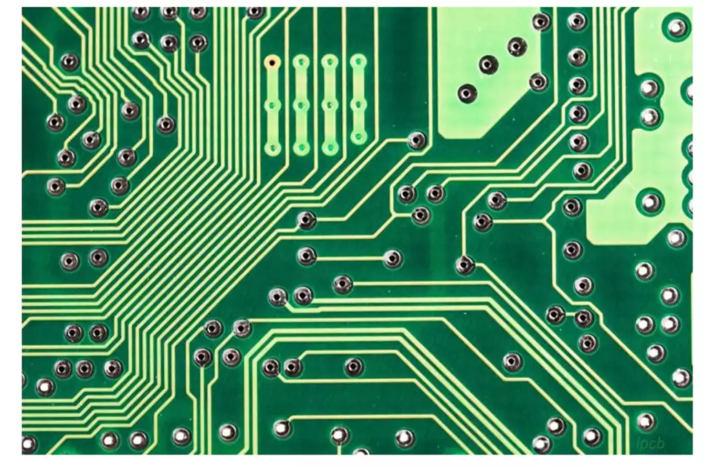
- Electrical connections: Inside the chip are many tiny electronic components, such as transistors and capacitors, which need to be connected to external circuits. The semiconductor Packaging process usually includes connecting the metal pads on the chip to the pins of the package via wires or other connections to the external circuitry.
- Heat dissipation: The package also helps dissipate the heat generated by the chip to the external environment to prevent overheating from affecting the performance of the chip.
- Protection: Packages provide environmental protection for semiconductor devices from dust, moisture and chemicals.
The choice of package usually depends on the specific application requirements, and different package types are suitable for different scenarios. Some common package types include Chip-Scale Package (CSP), QFN Package (Quad Flat No-leads Package), BGA Package (Ball Grid Array Package) and so on.
Semiconductor packaging process mainly includes wafer thinning, chip dicing, chip placement, chip interconnect, moulding and curing, de-flying burrs, soldering, coding, rib-cutting and moulding, appearance checking, finished product testing and semiconductor Packaging out of the warehouse and other key links, which cover a number of processes such as front-channel, middle-channel, electroplating, back-channel and final testing.
Wafer Thinning
Wafer thinning, also known as backside lapping, refers to the fine grinding of the backside of a wafer to achieve the required thickness for semiconductor Packaging. During the grinding process, protective tape is applied to the front side of the wafer to protect the circuit area. After grinding, the tape is removed and the thickness of the wafer is accurately measured.
Chip Dicing
Chip dicing, or wafer dicing, is divided into three sub-steps: wafer mounting, wafer dicing, and wafer cleaning. First, the wafer is securely taped to the blue film to prevent it from falling apart during dicing. Next, a saw blade is used to cut the entire wafer into individual chips. Finally, the wafer is cleaned to remove the dust generated during the cutting process to avoid affecting the subsequent processes.
Chip Mounting
After the chip cutting is completed, a second optical inspection is performed, i.e., the appearance of the cut wafer is inspected to identify the presence of scrap. After confirming that there is no scrap, enter the chip mounting section, which contains three steps: point silver paste, chip bonding and silver paste curing. Silver paste needs to be stored at a low temperature of -50℃, and it needs to be rewarmed and air bubbles removed before use. Curing of the silver paste is carried out at 175°C for 1 hour in an ammonia atmosphere to prevent oxidation.
Chip Interconnect
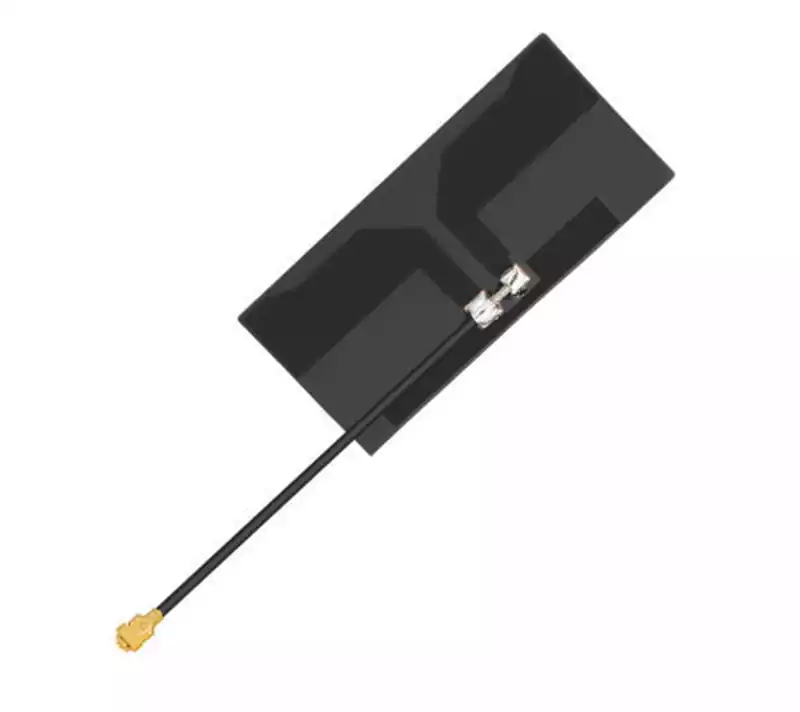
Chip interconnect technology is designed to connect the chip solder regions to the leads of the package enclosure or to the metal wiring solder regions on the substrate, thus enabling the function of the chip. This technique covers the physical connections between chips, between chips and package substrates, and between devices and substrates. Common chip interconnect methods include lead bonding, carrier tape auto-bonding and flip chip bonding (C4-Controlled Collapse Chip Interconnect).
Moulding and curing
Chip interconnects are followed by moulding and curing steps, including injection moulding and post-mould curing. Injection moulding uses a black block sealer, which is similar to silver paste, and needs to be stored at low temperatures and rewarmed for use. The sealer melts and then hardens at elevated temperatures and is typically moulded in 60 to 120 seconds. To do this, the leadframe is placed in the mould, ensuring that the chip is in the cavity, and then the plastisol is inserted, which melts and covers the chip from the bottom. Post-mould curing is done by curing the product at 175±5°C for about 8 hours to protect the internal structure of the IC and remove internal stresses.
Deburring
After the injection moulding is completed, excess sealing material may remain on the surface of the product, which needs to be deburred, i.e. de-spill process. This step through the weak acid solution immersion, so that the overflow part of the chemical corrosion, weakening its bonding force, and then through the high-pressure water rinsing, completely remove the excess material, so that the appearance of the product to meet the clean standards.
Soldering
The soldering process is immediately followed by electroplating. The electroplating process utilises the principles of electrochemical or chemical deposition to form a uniform and dense metallic coating on the surface of the leadframe. This layer of plating can effectively resist humid air, high temperature and other external environmental erosion, and improve the components and printed circuit board (PCB) welding suitability, reduce contact resistance, enhance electrical conductivity.
Current plating technology is mainly divided into lead-free plating and lead-tin alloy plating two categories. Lead-free plating uses high-purity tin with a purity of more than 99.95% as the plating material, which complies with the ROHS environmental directive and is widely used in the manufacture of electronic products. Lead-tin alloy plating has been gradually eliminated from the market due to the fact that its alloy composition contains 15% lead and 85% tin, which is not in line with environmental norms.
After plating, an annealing process is required. The lead-free plated product is baked at a high temperature of 150±5°C for a specific period of time to release the internal stresses of the plating layer and inhibit the risk of whisker growth. Whiskers are needle-like crystals that form on the surface of the metal plating and can cause short circuits if allowed to grow, and the annealing process eliminates this risk and ensures long term stable operation of the product.
Coding
The coding step, also known as laser typing, is a process whereby important information such as product name, date of manufacture and batch number is clearly engraved on the back or front of the product by means of laser technology.
Cutting and forming
Cutting and forming consists of two steps: cutting and forming. Trimming is the precise cutting of a whole lead frame into individual units. Forming is the process of pinning the cut IC product to the specific shape required by the process, and then placing the formed product into a tube or tray. Afterwards, the third appearance inspection, the fourth optical inspection, is carried out, using a low magnification lens to fully inspect the appearance of the product, focusing on the detection of injection moulding defects, plating defects, and rib-cutting/moulding defects.
Finished Product Testing and Packaging
After completing the appearance inspection, finished product testing will be carried out to ensure that the product meets the quality standard by carrying out comprehensive and strict testing of various performance indexes of the product. Finally, the tested products will be carefully packaged and shipped out according to the relevant procedures, ready to be delivered to customers.
Semiconductor packaging is the final part of the integrated circuit manufacturing, the core of which is the tested wafer processing into an independent, fully functional chip. Initially, packaging is mainly responsible for fixing the chip, providing electrical connection and protection, however, with the post-Moore’s Law era of higher requirements for chip performance, power consumption and integration, advanced packaging technology came into being, blurring the boundaries of the front-channel and back-channel processes, and has become an important direction to enhance the system arithmetic power and optimise the interconnectivity of the chip.