Introduction
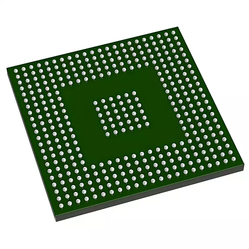
What is solder mask in pcb? Solder mask is a thin layer of polymer placed on the circuit board to protect the copper from oxidation and short circuits during operation. It also protects the PCB from environmental effects.
For example: dust and several other contaminants, which may cause short circuits in the long run.
Types of PCB solder mask
Top and bottom solder mask
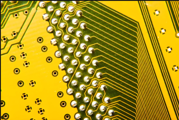
Engineers usually use these to identify openings in the green solder mask that has been applied on the PCB. This special solder mask is added through epoxy or film methods. Next, the component pins are soldered to the board using the openings that have been registered using the mask.
The traces on the top of the circuit board are called top traces, and the corresponding solder mask used is called the top mask. Same as the top mask, the bottom mask is used for the bottom of the circuit board.
Epoxy liquid solder mask
The most cost-effective choice in solder mask is epoxy. It is a polymer that is screen printed on the PCB. Screen printing refers to a printing technique that uses a woven mesh to support the ink blocking pattern. The grid is able to identify the open areas for the ink transfer process. This step is followed by heat curing
Liquid Photoimageable (LPI) Solder Mask
LPI solder mask is actually a mixture of two different liquids. These liquids are kept separately and mixed before applying the mask layer to extend the shelf life. LPI is also one of the more cost-effective options among various other types.
Used in curtain coating, screen printing and spraying applications, LPI is a mixture of various polymers and solvents. A thin coating is formed using this mask that adheres to the surface of the target area. After applying this mask, the PCB usually does not require any of the currently available final surface treatments.
Unlike traditional epoxy inks, LPI is sensitive to UV light. The panel needs to be covered with a mask and after a short “tack cure cycle”, the PCB is exposed to UV light using a UV laser or photolithography process.
Before applying the mask, the panel is cleaned and inspected for any signs of oxidation. This is done using a chemical solution, an aluminum oxide solution or by scrubbing the panel using a suspended pumice stone.
One of the most popular techniques used to expose the panel surface to UV light is the use of a film tool and a contact printer. The top and bottom sheets of film are printed using emulsion to block out the areas that need to be soldered. The production panel and film are then held in place using tools on the printer and exposed to a UV light source simultaneously.
One method utilizes direct imaging using a laser. This technique does not require tools or films because the laser is controlled by using fiducial marks placed on the panel copper stencil.
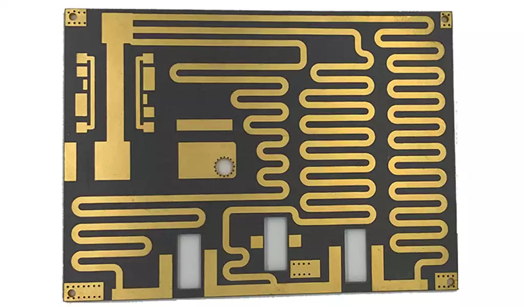
LPI masks are available in a variety of colors such as green, black, red, yellow, white, and blue.
Dry Film Photoimageable Solder Mask
The use of dry film photoimageable solder mask requires vacuum lamination, which is exposed and then developed. After development, openings are identified to generate a pattern, and components are then soldered to the copper pads. High density circuit boards benefit from dry film solder mask because it does not flood the through holes.
Surface Finish
Regardless of the PCB solder mask type used, the final solder mask will leave certain exposed copper areas on the board. These exposed areas need to be plated with a suitable surface finish to prevent oxidation. One of the most popular surface finishes is hot air solder leveling (HASL).
Other surface finishes such as electroless nickel palladium immersion gold (ENEPIC) and electroless nickel immersion gold (ENIG) are also available upon request. When required, additional holes are left in the mask layer for paste masks. This paste mask is used to connect pads or other components to the board depending on the manufacturing process used.
PCB solder mask production process
The following is the process of applying solder mask on PCB:
PCB cleaning
The circuit is cleaned to remove dirt and other contaminants, and then the surface of the board is dried.
Solder mask ink coating
Next, the board is loaded into a vertical coater for solder mask ink coating. The coating thickness depends on factors such as the reliability required for the PCB and its field of use. When solder mask is added to different parts of the board, such as traces, copper foil or substrate, its thickness will vary. This mask layer thickness will depend on equipment capabilities and PCB manufacturing capabilities.
Pre-hardening
This stage is different from full hardening because pre-hardening seems to make the coating relatively solid on the board, which helps remove unwanted coatings, which in turn can be easily removed from the PCB during the development stage.
Imaging and Hardening
Imaging is done using a laser-drawn photographic film to define the solder mask areas. This film is aligned to the panel that has been coated with solder ink and tacked dry. During this imaging process, the film aligned to the panel is exposed to UV light. After receiving the UV light, the opaque areas allow the UV light to pass through the film, which causes the ink underneath the opaque areas to polymerize (harden).
In the case of LDI imaging, no photographic film is required because the UV laser directly hardens the portion of the board where the solder mask ink needs to remain.
Development
The board is then immersed in a developer to remove the unwanted solder mask to ensure that the required copper foil is accurately exposed.
Final Hardening and Cleaning
Final hardening is required to make the solder mask ink usable when mounted on the PCB surface. Next, the board that has been covered with solder mask needs to be cleaned before further processing such as surface treatment.
Solder Mask Design Guidelines
Tented Via
When a via is covered with solder mask so that it is not exposed, it is called a tented via. Unlike via filling, here only the annular ring is covered by solder mask. If the hole is completely closed, it is called a filled via or a mask-plugged via, depending on the method used to close the hole.
Tented vias are a popular process used to protect PCBs, and are chosen over epoxy filling or mask plugging for cost considerations. Of the via bumping methods, liquid photo imaging (LPI) solder mask bumping is the most cost-effective.
To ensure better tented vias, you can also use a more costly resin fill.
The purpose of vias is to leave less exposed conductive pads on the PCB surface, which will minimize shorts that occur during solder bridging during assembly. When vias are located at the edge of the pad or in a standard BGA “dog bone” pattern, tin migration from the SMT pad is also reduced, and tenting can also minimize the possibility of vias being damaged by exposure to the operating environment.
Solder Mask Clearance
Solder mask clearance is the tolerance that determines how close the solder mask is to the surface features of the PCB. The purpose of this tolerance gap is to provide adequate spacing between surface features that receive solder, called solder dams. This prevents the formation of solder bridges.
Typically the solder mask gap needs to be half the conductor pitch width. When using fine conductive patterns below 100μm, the solder mask gap can be below 50μm.
Pads
Pads defined by solder mask are those pads where the mask opening is smaller than the copper pad, so that the solder mask will define the pad size used in the BGA.The variation in mask gap will determine the size of the copper pad.
Non-solder mask defined pads include the gap between the pad and the mask.
The solder mask process needs to take into account the fitting tolerance so that the mask gap should always be larger than the pad. This is necessary to keep the entire pad free of solder mask and ensure optimal soldering.
Solder Mask Opening
The outer layer of the PCB without a mask is called a solder mask opening, and its purpose is to expose the circuit to tin (solder). This opening must be accurate, otherwise it may result in unnecessary copper exposure on the board, which can cause corrosion and damage.
Usually, manufacturers choose to have a 1:1 solder mask opening to copper pads that can be changed for appropriate manufacturing processes. The opening must be customized as required, otherwise it may result in the ground plane next to the pad being exposed. This can cause shorts and should be prevented.
Solder Mask Coverage or Extension
EDA software often allows you to set the spacing between board surface features and the solder mask. This specification is often called solder mask extension and can be positive, negative, or zero.
Positive Solder Mask Extension
When there is spacing between the end of the solder mask and the outer circumference of the pad that is not covered, it is called positive solder mask expansion.
Zero Solder Mask Expansion
When there is no spacing or gap between the solder mask and the pad, it is a zero value.