The Nature and Formation Mechanism of Cold Solder Joints
In electronic manufacturing and soldering quality control, cold solder joints are a seemingly basic but long-underestimated hidden problem. It’s not a “rare defect,” but a common source of failure throughout the entire process of manual soldering, SMT assembly, wave soldering, and even rework. Many products perform normally during factory testing, but frequently experience intermittent failures during transportation, assembly, or early use; the root cause often lies in this incomplete soldering structure.
From a physical perspective, a cold solder joint refers to a solder joint that fails to receive sufficient heat or wetting conditions during the soldering process, resulting in the absence of a complete and stable intermetallic compound layer between the solder and the pad/lead. Superficially, the solder joint appears to be “glued,” but in reality, its internal structure is loose, with coarse grains and extremely weak interfacial bonding. At the microscopic level, this solder joint is not a continuous metal connection, but rather more like a contact point that has been “barely glued together.”
The root cause of this problem is often not a single factor, but the result of multiple process conditions combined. The most typical cause is insufficient soldering temperature or too short heating time, where the solder is removed or cooled before it is fully melted. Secondly, oxidation, contamination, or residual flux failure on the pads or leads prevents proper solder wetting of the metal surface. Furthermore, in SMT production, improper reflow profile design, mismatched heat capacity, and excessively rapid localized heat dissipation from components or the PCB all significantly increase the probability of cold solder joints.
It is important to note that cold solder joints do not necessarily appear as “obvious errors” in appearance. Unlike defects such as cold solder joints or bridging, they are often deceptive. Under optical inspection, these joints may still appear to be in a basic formed state, but the solder surface is dull, grainy, and the edges are not adequately wetted, resulting in an uneven joint outline. It is this “deceptive” appearance that makes them easily overlooked in early production stages, but exposes fatal problems in later reliability testing and field applications.
From an electrical performance perspective, the most dangerous characteristic of cold solder joints is their instability. In static testing, it may appear to have normal conductivity; however, under conditions of temperature changes, vibration, mechanical stress, or current fluctuations, microcracks within the solder joint will continuously expand, causing contact resistance to fluctuate, ultimately leading to signal jitter, intermittent open circuits, or even complete failure. This is why the tolerance for cold solder joint problems is almost zero in high-reliability fields such as automotive electronics, industrial control, and medical equipment.
Therefore, understanding the formation mechanism of cold solder joints is not simply about “identifying a defect term,” but rather laying the foundation for subsequent process control, design optimization, and the establishment of a quality system. Only by truly recognizing that it is a structural rather than a superficial problem can we systematically discuss how to prevent, detect, and minimize its risks at the design and manufacturing levels in later chapters.
Main Causes and Process Runaway Scenarios of Cold Solder Joints
In actual production, cold solder joints rarely occur “accidentally.” They are often the result of accumulated problems arising from a long-term neglect, simplification, or misjudgment of a certain link in the soldering system. Understanding the causes of cold solder joints cannot be limited to the superficial judgment of “insufficient temperature.” Instead, it requires analyzing the formation environment from four dimensions: heat, materials, time, and process synergy.
First, from a heat input perspective, soldering is essentially a controlled energy transfer process. Whether it’s manual soldering or SMT reflow soldering, the solder must fully melt within a suitable temperature range and remain in a liquid state for a sufficient time to form a stable intermetallic compound layer with the pads and device leads. If heating is insufficient, the solder, although softened on the surface, does not fully flow, resulting in a loosely structured solder joint upon cooling. This situation is very common in practice; for example, low soldering iron power, insufficient local temperature in the reflow oven, or excessive PCB heat capacity causing localized temperature lag can all directly induce cold solder joint problems.
Second, the time factor is often underestimated. Soldering is not an “instantaneous” process, especially in SMT reflow. The solder needs to remain in the liquid phase for a sufficient time to complete wetting, diffusion, and interfacial reactions. If the reflow profile is compressed to maximize production capacity, or the high-temperature period is deliberately shortened to protect components, the solder may begin to cool before the metallurgical bond is complete. The resulting solder joint may appear conductive in initial testing, but its internal structure already harbors reliability vulnerabilities.
Material factors are also a significant cause of cold solder joints. The surface condition of the pads directly determines the solder’s wetting ability. When PCB pads are oxidized, have been stored for too long, have contaminated surface treatments, or have uneven treatment layer thickness, the interfacial reaction between the solder and metal is significantly inhibited. Even if the temperature and time parameters seem reasonable, it is difficult to form a high-quality solder joint. This problem is particularly prominent in lead-free soldering systems because lead-free solder itself has weaker wetting properties and is more dependent on the pad condition and flux activity.
Furthermore, considering process coordination issues, cold solder joints are often not a single point of failure, but rather the result of multiple seemingly reasonable decisions combined. For example, choosing a PCB material with lower thermal conductivity to reduce costs; increasing copper thickness to control warpage; and lowering peak temperature to protect components. These adjustments, individually, may not seem obviously wrong, but without simultaneous optimization of reflow profiles or soldering strategies, they can create typical cold solder joint runaway zones in localized areas.
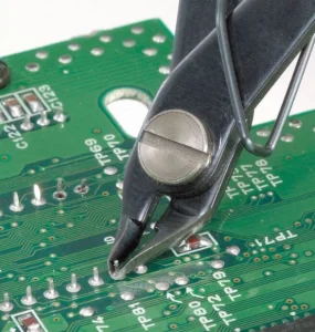
Furthermore, human factors are particularly critical in manual soldering and rework processes. Prematurely moving solder joints or applying mechanical stress before the solder has fully solidified can damage the forming metal structure, making the solder joint appear “complete” on the surface, while microcracks have already formed internally. These types of cold solder joints typically fail rapidly after vibration or thermal cycling, and are a significant cause of recurring failures after field rework.
In summary, the formation of cold solder joints is not due to a single parameter failure, but rather the result of insufficient heat input, timing mismatch, poor material condition, and process imbalance. Only by moving beyond the “single-point troubleshooting” mindset and re-examining the soldering process from a systemic perspective can the probability of cold solder joints occurring in production be truly reduced.
Long-term impact of cold solder joints on reliability and electrical performance
Of all soldering defects, the danger of cold solder joints lies not in their frequency of occurrence, but in the extreme difficulty of being fully detected by a single test. Many electronic products function perfectly at the factory, but develop malfunctions during customer use. The root cause often lies in the structurally incomplete solder joints. Cold solder joints are not a matter of “immediate failure,” but rather a typical delayed reliability risk.
Structurally, the internal metal structure of cold solder joints typically exhibits coarse grains, numerous pores, and discontinuous interface bonding. While this structure can maintain basic conductivity under static conditions, in real-world applications, once subjected to temperature changes, mechanical vibrations, or thermal expansion and contraction, the stress within the solder joint concentrates at those already weakened interface locations. Over time, microcracks propagate, eventually evolving into visible cracks or even complete fracture.
From an electrical performance perspective, the biggest problem with cold solder joints is the instability of contact resistance. Compared to normal solder joints, the contact interface of cold solder joints is not continuous and uniform; its resistance value often fluctuates with temperature and mechanical conditions. In low-speed or low-power applications, such changes may go unnoticed temporarily; however, in high-speed signal, radio frequency applications, or high-current scenarios, even minute impedance changes can trigger signal distortion, increased jitter, or even direct communication failures or system restarts.
More deceptively, these problems often present as “intermittent failures.” The device operates normally under certain conditions, but suddenly fails after vibration, temperature increases, or prolonged operation, only to recover after a restart or slight movement. This uncertainty not only greatly increases the difficulty of fault localization but also severely impacts end-users’ trust in product stability. Once in the field application phase, troubleshooting costs often far exceed prevention costs during the manufacturing phase.
In reliability testing, cold solder joints are also among the defects most easily amplified. Thermal cycling, high and low temperature shocks, vibration testing, and mechanical stress testing all rapidly expose structural defects in cold solder joints. Many products that “pass” functional testing at room temperature experience batch failures in reliability testing; the root cause is not design flaws but rather solder joint quality failing to meet long-term service requirements.
From a system perspective, cold solder joints can also trigger a cascading failure risk. An unstable solder joint not only affects the devices it connects to but can also lead to localized overheating and abnormal current distribution, thereby accelerating the aging of surrounding solder joints and devices. In highly integrated or high-value systems, the losses caused by this chain reaction often far exceed the repair cost of a single solder joint.
Therefore, a cold solder joint is not a minor defect that can be “tolerated,” but a structural problem that amplifies over time and under stress. A truly mature manufacturing system must treat it as part of reliability design, not simply a cosmetic or manufacturing defect.
A Systematic Prevention Approach from Design to Manufacturing
A truly mature electronic manufacturing system does not wait until a cold solder joint appears to repair it, but rather manages it systematically as a foreseeable and controllable risk in the early stages of design and manufacturing. The recurrence of cold solder joints is often not due to uncontrollable technology, but rather to a lack of preventative mechanisms or inconsistent implementation.
During the design phase, the impact on soldering reliability is often underestimated. Pad size, copper thickness distribution, via location, and the thermal diffusion effect of large-area copper foil all directly affect the heat uniformity of local solder joints. When the heat capacity of a certain area is significantly higher than that of the surrounding areas, even if the overall reflow profile meets specifications, the solder joints in that area may not receive sufficient heat, leading to a potential risk of cold solder joints. Therefore, it is necessary to predict the thermal balance during the layout phase and, if necessary, reduce the impact of local temperature differences on soldering quality through thermal isolation design, adjustment of pad structure, or optimization of copper distribution.
In the manufacturing stage, the stability of the reflow soldering process is one of the core factors in preventing cold solder joints. A reasonable reflow profile must not only meet the solder melting point requirements but also take into account the differences in thermal response between different components and PCB areas. Especially in the case of multilayer boards, high copper thickness, or mixed components, a single “universal profile” often cannot cover all solder joints. Ensuring sufficient and uniform reaction time for the solder in the liquid phase region through actual temperature measurement and dynamic adjustment of temperature zones and transfer speed is an important prerequisite for reducing cold solder joints.
Material management is equally crucial. The surface treatment of the pads, the storage conditions of the solder paste, and the activity of the flux all directly affect the soldering wetting effect. Even with reasonable process parameter settings, cold solder joint problems are still difficult to avoid if the material condition is unstable. Therefore, establishing comprehensive incoming material inspection and storage standards, ensuring solder paste is used within its expiration date and in a suitable environment, and strictly controlling pad oxidation and contamination are fundamental conditions for preventing cold solder joints.
At the quality control level, relying solely on visual inspection is often insufficient to detect potential risks. Cold solder joints exhibit a clear “delayed failure” characteristic, requiring early identification through process monitoring and reliability testing. Combining SPI, AOI, and sampling functional and environmental stress testing can identify weaknesses in the soldering system before mass production, rather than leaving risks to be exposed at the customer’s end.
Furthermore, standardized management of human factors is equally important. Whether it’s manual soldering or rework, the soldering personnel’s understanding and adherence to process standards directly impacts solder joint quality. Systematic training, standardized operating procedures, and key process review mechanisms can significantly reduce cold soldering problems caused by differences in operating habits.
In summary, preventing cold solder joints is not the responsibility of a single position or process, but rather a systematic project spanning the entire process of design, process, materials, and quality management. Only by viewing soldering reliability as part of product value, rather than merely a manufacturing detail, can cold solder joints be truly kept within acceptable limits.
Summary
Why Cold Solder Joints are the Most Expensive Hidden Risk in Electronics Manufacturing
As can be seen from the preceding text, cold solder joints are not a “low-level but insignificant” process defect, but rather a highly destructive structural risk. They often don’t surface during factory testing but gradually amplify during critical stages of the product lifecycle, ultimately manifesting as unstable failures, field failures, or even system paralysis.
From a formation mechanism perspective, cold solder joints are not accidental but the result of multiple factors, including insufficient heat input, imbalanced timing control, unstable material conditions, and insufficient design and process coordination. From an impact perspective, they directly weaken the mechanical strength and electrical stability of the solder joint, continuously deteriorating under temperature changes, vibration, and long-term operating stress, becoming a typical source of delayed failure.
More importantly, the cost of cold solder joints is not limited to rework or scrap costs. It also consumes significant engineering resources for troubleshooting, undermines customer trust in product reliability, and introduces incalculable brand risks in high-reliability applications. Therefore, treating cold solder joints as part of a reliable design and manufacturing system, rather than simply a process issue, is a crucial step in transitioning electronics manufacturing from “usable” to “reliable.”
Truly mature manufacturing capability lies not in the ability to repair cold solder joints, but in the ability to systematically prevent and eliminate them in the early stages of design and manufacturing.