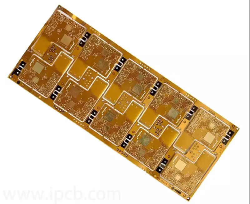
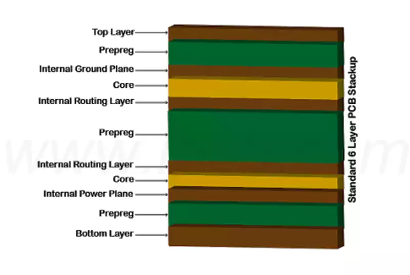
A 6 layer pcb stackup structure is a design in which six layers of conductive and non-conductive materials are stacked together during the circuit board manufacturing process to achieve complex circuit connections. This type of structure is commonly used in electronic products that require high-density wiring and multifunctional integration.
Common 6 layer pcb stackup:
- SIG-GND-SIG-PWR-GND-SIG;
The advantage of this stacking scheme is that better signal integrity can be obtained, the signal layer is adjacent to the ground layer, the power and ground layers are paired, the impedance of each alignment layer is relatively easy to control, and the arrangement of the two ground layers provides better absorption of the magnetic field, and provides a better return path for each signal layer in the case of a complete power ground layer.
2.GND-SIG-GND-PWR-SIG-GND
It should be noted that this stacking scheme is only suitable for the case of low device density, the advantage is that it has all the advantages of the above stacking, and the ground plane of the top and bottom layers is relatively complete, which can be used as a shielding layer. In addition, the power supply layer of the stacking method needs to be close to the main components of the more of the layer, because the bottom layer of the plane will be more complete, so the EMI performance is better than the first.
6 layer pcb stackup design rules:
- Preferred ground plane: Ground planes are the best choice because they efficiently carry signals in the stripline. This is critical for reducing ground noise, as lower ground impedance significantly reduces this noise.
- High-speed signals are placed in the middle layer: High-speed signals should be directed between the layers of the PCB, especially the middle layer. In this way, the ground plane can play an effective shielding role, inhibit the signal to the fastest speed propagation of radiation.
- Signal layer adjacent to the ground plane: The signal layer should be as close as possible to the ground plane to optimise signal transmission and reduce interference.
- Careful connection of power and ground planes: Special care needs to be taken when connecting power and ground planes to ensure good electrical performance and stability.
- Ensure symmetrical stacked-layer configuration: The stacked-layer design should be kept as symmetrical as possible to reduce the impact of thermal and mechanical stress on the PCB.
- Meet signal impedance requirements: The design should ensure that the required signal impedance is met to ensure the quality and integrity of signal transmission.
- Consider the thickness of the signal layer: the thickness of each signal layer is an important factor in the design, and the appropriate standard thickness should be selected according to the characteristics of the PCB material used.
- Focus on material quality: In addition to considering the intended use of the material, close attention should be paid to its mechanical, chemical, electrical and thermal properties to ensure the quality and performance of the PCB.
- Optimise the return path: When the signal level is close to the plane (ground or power) level, the return current can flow in adjacent planes, thus minimising the inductance of the return path.
- Thinning the insulation layer to improve performance: the signal layer and its adjacent planes between the insulation layer can be designed thinner to improve noise suppression and EMI (electromagnetic interference) performance.
When designing a 6 layer pcb stackup, the following key factors need to be considered:
Signal Integrity Elements
The effect of electrical signal transmission on the circuit board is directly related to signal integrity. Therefore, fine planning of trace lengths becomes critical to prevent signal delays and distortions. On the other hand, impedance matching strategies require traces and terminations to be designed to match the characteristic impedance of the transmission line, thus minimising signal reflections. Additionally, minimising crosstalk between adjacent lines is essential to avoid interference and safeguard signal integrity. By addressing these factors, the design maintains the required signal quality and prevents data errors or signal degradation.
Determining a single power reference plane (i.e., power plane)
Determining a single power reference plane is one of the key steps in safeguarding power integrity, and the use of decoupling capacitors plays an important role in this process. In order to effectively maintain power integrity, decoupling capacitors need to be arranged according to strict rules: they can only be placed on the top or bottom layer of the PCB. The connection details of decoupling capacitors, including alignments, pads and vias, can have a significant impact on their performance. Therefore, when designing, it is important to make sure that the alignment of the decoupling capacitors is as short and wide as possible, and that the wires to the vias are kept to a minimum length.
In the case of high-speed digital circuits, for example, the following strategy can be adopted: place the decoupling capacitors on the top layer of the PCB, designate layer 2 as the dedicated power supply layer for high-speed digital circuits (e.g., processors), use layer 3 as the signal layer, and set up layer 4 as the working level of the high-speed digital circuits again.
In addition, to ensure signal alignment stability, we should try to have signal alignments driven by the same high-speed digital device share the same power supply layer as a reference plane, and this power supply layer should be the same layer that provides power to the high-speed digital device.
Impedance Control and Cabling Specifications
Impedance control and cabling specifications play an important role in ensuring consistent signal characteristics and preventing signal degradation. These specifications define specific requirements for wire width, spacing, and layer stacking to achieve target impedance values. Following these specifications helps to minimise reflections and signal distortion.
EMI/EMC Concerns
EMI/EMC considerations are critical to minimising electromagnetic interference and ensuring compliance with electromagnetic compatibility standards. The use of shielding techniques, proper grounding strategies, and strategic placement of components are key to mitigating EMI/EMC issues and ensuring stable operation of the printed circuit board in its intended environment.
Material Selection
Standard substrate materials or aluminium cores can be used for the fabrication of single-layer printed circuit boards. However, for multi-layer stacked boards, aluminium core printed circuit boards are clearly not suitable due to the challenging manufacturing process of multi-layer aluminium printed circuit boards.
The 6 layer pcb stackup design is the key to complex circuit connections in electronic products, and requires comprehensive consideration of signal integrity, power integrity, impedance control, cabling specifications, and EMI/EMC to ensure the high performance and reliability of the design.