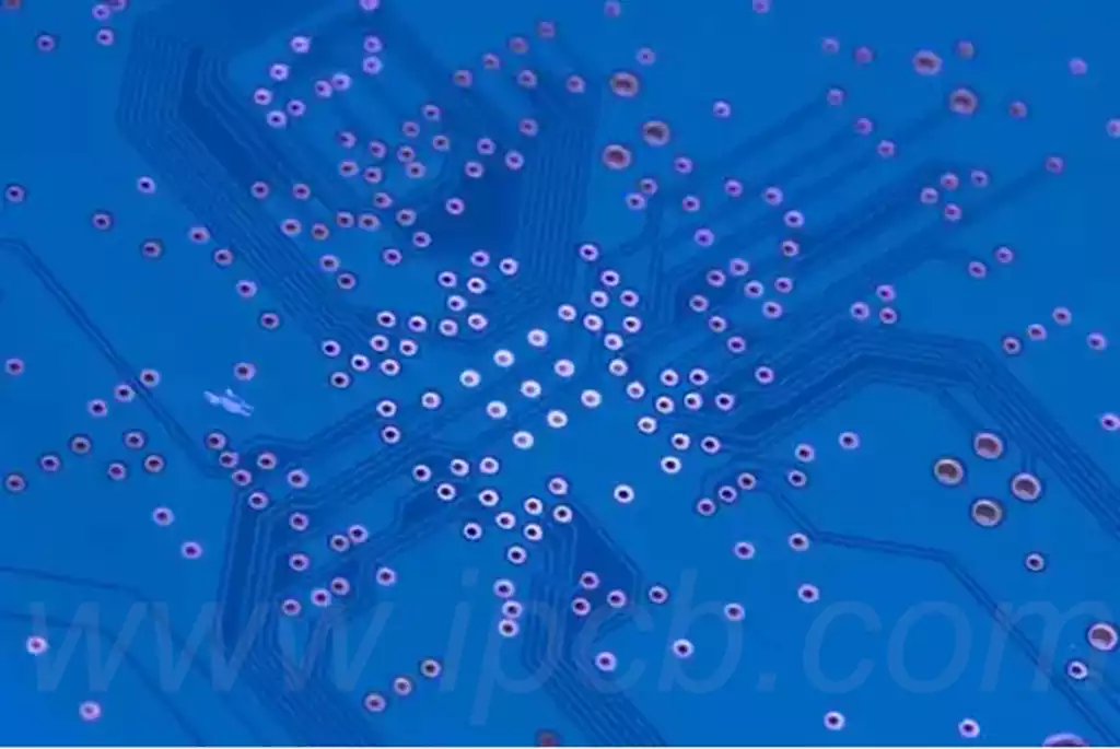
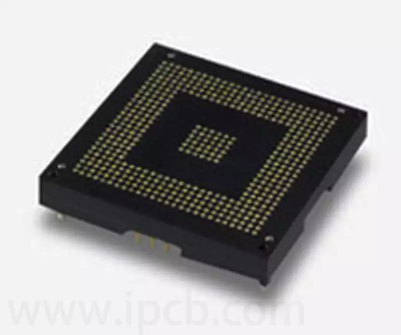
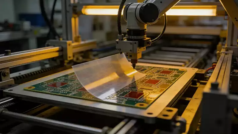
ENIG Finish PCB is printed circuit boards (PCBs) that are finished using the ENIG (Electroless Nickel Immersion Gold) process. This process is characterized by the uniform deposition of a layer of nickel on the copper surface of the board through a chemical reaction, followed by immersion in a gold solution to form a thin, uniform layer of gold. This structure gives ENIG Finish PCBs the advantages of high strength and low contact resistance, so they are widely used in a variety of high-end electronic products, such as PCBA boards for cell phone internals and BGA carrier boards.This surface treatment ensures that electronic products work stably and reliably in a variety of environments and applications.
ENIG (Electroless Nickel Immersion Gold), is a surface treatment for circuit boards (Finished) process,generally referred to as electroless nickel immersion gold board or simply referred to as the gold board, is now widely used in cell phones mounted on PCBA boards,some BGA carrier boards will also use ENIG.
One of the biggest advantages of ENIG surface treatment circuit boards is that the pcb board production and manufacturing process is simple, in principle, you only need to use two chemical potions (chemical nickel plating and acidic gold water) can be completed, of course, there is also a need for other potions to assist.ENIG surface treatment process is generally the first in the copper pads made of chemical nickel deposition, through the control of the time and temperature to control the thickness of the nickel layer,and then use the fresh just deposited to complete the fresh Then, using the freshly deposited nickel activity,the nickel pads are immersed in acidic gold water,and the gold is replaced from the solution to the surface of the pads through a chemical replacement reaction, while part of the surface of the nickel is dissolved into the gold water.The replaced “gold” will gradually cover the nickel layer until the nickel layer is completely covered, the replacement reaction will automatically stop,cleaning the pad surface dirt after the process can be completed. At this point,the gold layer is often only about 0.05um (2u”) thick or thinner,so the ENIG process is very easy to control and relatively low cost (compared to electroless nickel gold plating).
Obviously the surface of this thin layer of gold can only play a role in the oxidation of the nickel layer of protection,once the gold layer is not enough to protect the nickel layer, resulting in corrosion and oxidation of nickel in contact with the air or by the transition of the gold leaching,that is,the formation of the so-called “black nickel” or “black pads” phenomenon, and at this time,the surface of the pads appear to the naked eye is still golden gold,generally visually it is very difficult to determine whether or not there is a problem.Therefore,it is very necessary to strengthen the quality inspection of ENIG surface-treated PCBs before the assembly process.
Compared to electroplating nickel gold, this nickelized immersion gold in the circuit board manufacturer’s process does not need to be electrified on the circuit board, and does not need to be plated on each of the pads to be pulled above a wire to connect to the nickel gold plating, so its process is relatively simple, the yield is also a multiple of the above, so the cost of production is also relatively inexpensive.
The immersion gold process stands out in PCB manufacturing for its excellent flatness and versatility. The flatness of the pad surface is one of the key factors in ensuring the stability and performance of electronic component connections.
Not only that, a flat pad surface also helps to reduce soldering stresses and improve the reliability of electronic products. The gold deposition process can deposit a layer of nickel and gold evenly on the surface of the pads through precise chemical methods, making the surface smooth and flat.
The flatness of the pad surface is critical for all types of connections, especially in the manufacture of microelectronic devices and high-density integrated circuits. Whether it is traditional fusion welding, or the more complex lap or wire bonding (bonding), the immersion gold process provides the ideal foundation for these connection methods.
When soldering, the flat surface ensures an even distribution of solder, resulting in more reliable joints and connections. In lap welding or wire bonding, the flatness of the immersion layer provides a stable support platform for the wire, ensuring precise positioning of the joint and a high-quality connection.
In addition, the immersion gold layer serves as a superior protective layer, forming a solid barrier on the surface and sides of the pads, effectively blocking oxygen, humidity and chemicals from the outside world. This not only extends the life of the pad, but also improves component stability and reliability. In extreme environments, such as high temperatures, high humidity or corrosive gases, the protection provided by the immersion layer is particularly significant, providing a strong defense for electronic components.
The immersion gold process not only improves soldering quality and connection stability by ensuring the flatness of the pad surface, but also gives PCBs a wider range of application flexibility. Whether it is traditional soldering methods or more advanced connection technologies, immersion gold provides a solid foundation for outstanding performance in a variety of fields.
However, ENIG surface treatment also has its drawbacks and problems, such as low solder strength, easy to generate black pad (Black pad) is often criticized.
The production process of chemical nickel-gold is roughly as follows:
Pre-treatment → degreasing → washing → pickling → washing → micro-etching → washing → pre-impregnation (H2SO4) → activation (Pd catalyst) → washing → chemical nickel (Ni/P) → washing
Electroless Nickel Immersion Gold (ENIG) printed circuit boards have a wide range of applications in the electronics industry.Due to their high surface flatness, excellent solderability, and strong corrosion resistance,these boards are especially suitable for boards with high precision requirements. They are used in a wide range of high-end electronic products.
Mobile devices: In the production of mobile devices such as cell phones and tablets, these specially treated pcb boards are favored for their outstanding performance and reliability.
Medical technology: In view of the stringent requirements for component stability and reliability in medical equipment, these surface-treated circuit boards ensure the proper functioning of the equipment at critical moments, thus safeguarding the safety of patients.
Aerospace: In the aerospace sector, equipment is often operated under extreme environmental conditions. As a result, higher requirements are placed on the corrosion resistance and mechanical strength of the circuit boards. Electroless nickel-impregnated gold-plated boards are ideally suited to meet these demanding conditions.
Other high-end applications: In addition, printed circuit boards with this finish are used in many other high-end applications, from industrial controls to automotive electronics to telecommunications equipment.
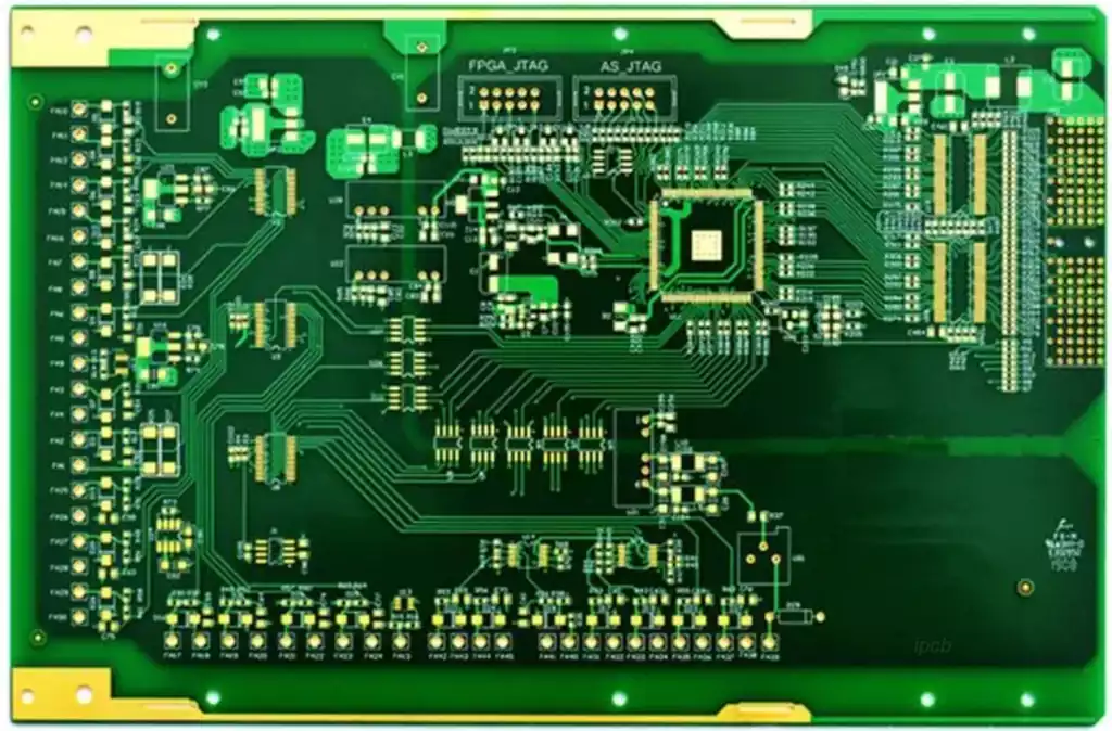
Advantages of ENIG (electroless nickel immersion gold) surface treatment for circuit boards:
The surface treatment can be used as a base metal for COB wiring.
Can be repeated many times reflow (reflow), generally requires at least 3 times more than the high-temperature welding, and welding quality can be maintained consistently.
Excellent conductivity.It can be used as a gold finger line for button conduction and has high reliability.
Gold metal activity is low,and not easy to react with atmospheric components, so it can play a certain anti-oxidation and anti-rust ability. So ENIG’s preservation period can easily exceed six months or more, sometimes even if placed in a warehouse for more than a year,as long as its preservation status is good, no rust problem,and the circuit board after baking and dehumidification and welding test confirmed that there is no problem,you can still continue to use to weld production.
Gold is not easy to oxidize when exposed to the air, so you can design a large area of exposed pads to be used as “heat sinks”.
It can be used as the contact surface of the blade plate. The gold plating must be thicker for this application.Hard gold plating is generally recommended.
ENIG has a flat surface, which makes it easy to print solder paste with good flatness and easy to solder.Ideal for fine interleafing parts and small parts such as BGA, Flip-Chip, etc.
ENIG limitations:
- Black pad:
ENIG finish PCB surface in the ENIG or welding process is prone to black disk effect (Black pad), which occurs in the Ni and gold junction surface, the direct expression of excessive oxidation of Ni. - Brittle gold
Too much gold (2 – 7Wt%), will make the solder joints brittle (brittle gold phenomenon), affecting reliability.
3.IMC
Nickel-tin intermetallic compounds than copper-tin intermetallic compounds with low strength, so the relative brittleness of nickel-tin intermetallic compounds will appear at a lot of problems.
ENIG Finish PCB is printed circuit board with excellent corrosion resistance, electrical conductivity, and solderability made using a chemical nickel layer and a gold immersion layer treatment process. It is an indispensable part of modern electronic manufacturing, providing a strong guarantee for the stable and reliable operation of various high-end electronic products.
