Solder pads are pieces or layers of metal on a circuit board that are used to solder electronic components to connect the circuitry on the core to the pins of the encapsulated chip grid. They are the bridge between the board and the components, connecting them together through soldering to ensure that the current can flow smoothly. The design and manufacturing quality of the pads are directly related to the reliability and performance of the circuit board.
Classification of solder pad design in PCB
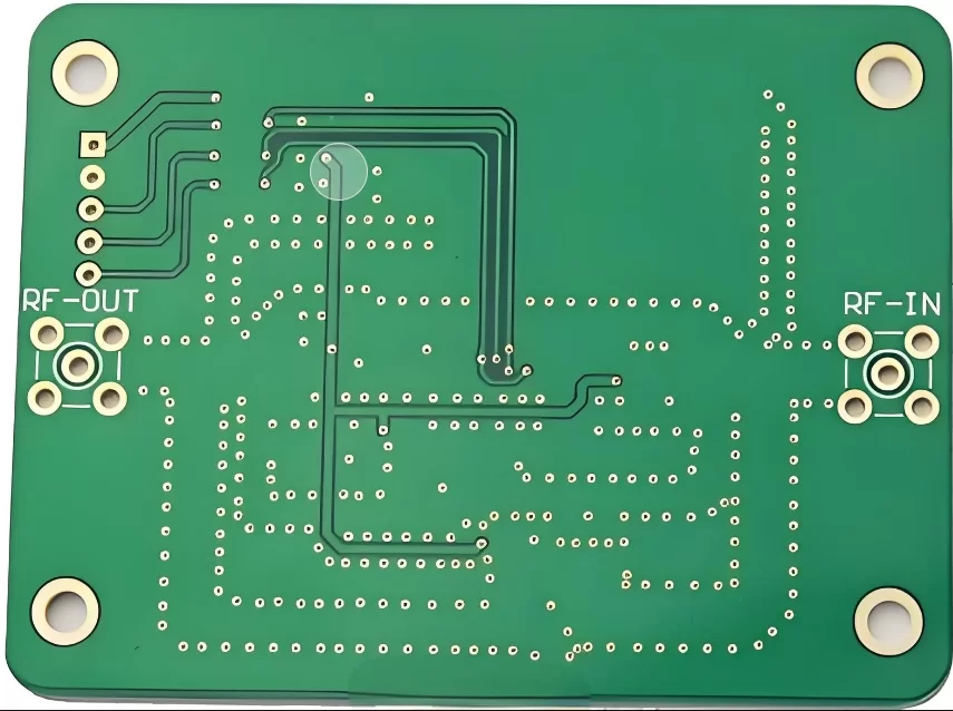
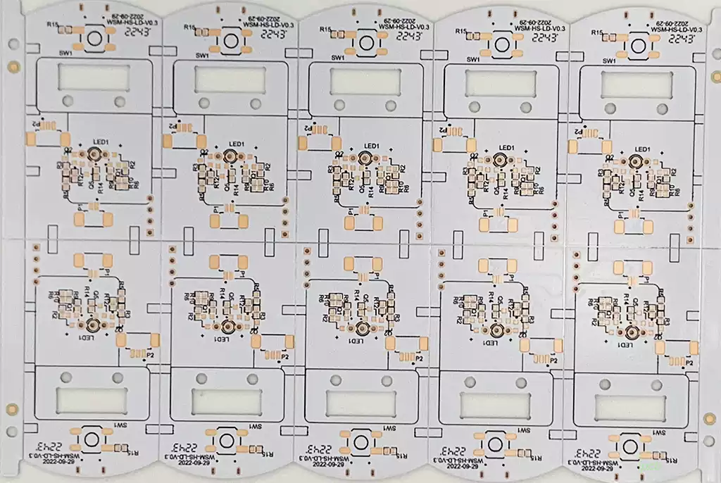
Surface Mount Pad
1) The pads used to mount surface mount components are called surface mount pads.These pads have the following characteristics: pads that show copper area. This can be rectangular,circular,square or rectangular among other shapes.
2) Solder resist layer
3) Solder paste
4) Pad number (number of pads present in the assembly)
Through-Hole Pad
The pads used to mount through-hole components are called through-hole pads and there are two types:
1) Plated Through-Hole (PTH)
PTH refers to pads with through holes, the walls of which are plated with copper and sometimes with solder or other protective plating. Hole plating is accomplished using an electrolytic process, and the plating provides an electrical connection between the different layers of the board.
2) Non-Plated Through Hole (NPTH)
NPTH is a pad that has no plating in the hole. The solder pads are primarily used for single panels or these holes are used to mount the pcb board in the enclosure and to mount screws through these holes. Typically, unplated holes do not have any copper in the area around the hole (similar to a board edge gap), this is done to prevent short circuits between the copper layer and the component to be placed.
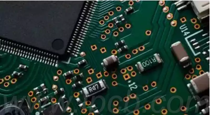
The different parts of a through-hole pad are often referred to as the pad stack and include:
Top pad
Bottom pad
Inner pad
Drill head
Ring
Pin numbering
Some of the major problems that can result from incorrectly sized pads:
Poor soldering: A solder pad size that is either too large or too small can lead to poor soldering. If the pad size is too large, too much solder buildup may form during soldering, resulting in unstable solder joints or short circuits. On the other hand, if the pad size is too small, it may not be able to hold enough solder, resulting in weak or false soldering.
Component Instability: Improperly sized pads may also result in unstable placement of electronic components on the board. A pad that is too large may cause the component to move during the soldering process, while a pad that is too small may not provide enough support, making the component susceptible to dislodgement or displacement.
Thermal Performance Issues: Pad size also has an effect on the thermal performance of the board. Pad sizes that are too large may increase heat buildup at the solder joints, leading to increased thermal stress, which can increase the risk of component damage. Pad sizes that are too small, on the other hand, may not be able to dissipate heat efficiently, again causing damage to components and boards.
Reduced electrical performance: Incorrectly sized pads can also affect the electrical performance of the board. For example, pads that are too small can lead to high current densities, increasing resistance and heat generation, which can affect signal transmission and overall performance.
Reduced productivity: Incorrectly sized pads can also lead to reduced productivity. During the production process, if the pads are not the right size, additional processes or adjustments may be required to ensure solder quality, which not only increases manufacturing costs, but may also affect the production schedule.
Solder pad as the electronic world in the “hidden hero”, although the name is not conspicuous, but its role can not be ignored. They silently bear the burden of current transmission to ensure the stable operation of electronic equipment.