PCB circuit board blind vias are holes in multilayer circuit boards that are used to connect different levels of internal lines, but do not run through the entire plate. Blind vias play an important role in increasing line density, reducing board size and enhancing circuit performance. Blind buried blind holes is a multilayer circuit board, the aperture of the blind holes in the internal welding electrical connection to realize the multilayer circuit board internal circuit connection.
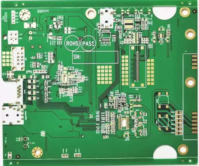
Characteristics of Blind Vias PCBs
Blind Via PCBs have significant differences compared to common PCB types and have various characteristics that make them unique compared to other types of printed circuit boards. For example, Blind Via PCBs use multiple layers on a single board, which makes them unique compared to regular PCBs that use only a single board without layering. The following are the characteristics of a blind vias PCB:
It uses different combinations of vias such as blind vias, buried vias and through vias. The reason for this is that blind vias cannot work without combining buried and through-hole connections. Blind vias need to connect buried vias and through vias so that multiple layers of the board can be connected together.
A blind vias PCB or HDI board has multiple layers. It uses an underlay connection system that allows the board to connect multiple layers into an interconnect circuit. This allows you to use the layering process to combine various components on a single board instead of using multiple boards to achieve the same result.
It connects components from different layers through an underlay connection. Blind vias connect components using only the bottom layer connections. Only the top side of the through-hole is visible from the board surface. The rest of the connections of the blind vias exist in the inner layers on the board.
The manufacturing process for PCB blind vias is roughly as follows:
(1) Pre-processing. The PCB is embossed with a photosensitizer and then process steps such as exposure and development are used to create the desired graphic traces.
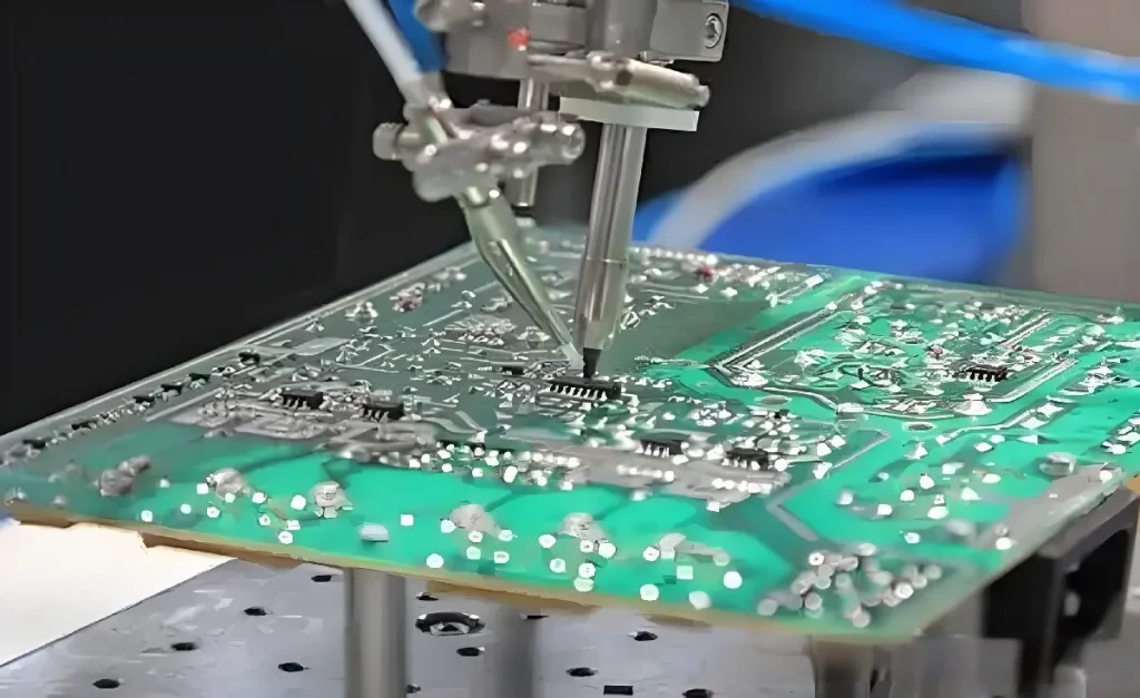
(2) Cooling drilling. Drill holes by cooling the drill bit on the blind hole position, and form the blind hole aperture by controlling the depth and diameter of the drill hole.
(3) Copper plating. The PCB is placed in a copper electrolyte and a copper source is deposited on the PCB substrate surface through an electrochemical reaction to form a copper film of the desired thickness.
(4) Bonding process. The board to be buried with holes is bonded to other boards or substrates using a pressure-sensitive adhesive, which is then heated to cure the pressure-sensitive adhesive.
(5) Copper plating of buried holes. The board containing the blind holes is copper-plated again to form a conductive layer inside the blind holes.
(6) Debonding and Stripping. The pressure-sensitive adhesive on the board is stripped using a chemical agent to form a non-conductive area around the blind hole.
(7) Final adjustment processes, including gold immersion, embossing, cutting and stacking, resulting in the final PCB blind hole board.
PCB blind hole is a complex manufacturing process, need to pay attention to the following process points:
(1) Drilling technology. PCB blind vias cannot be manufactured without cooling drilling technology, because high-speed drilling will cause the deposition of fine cracks on the surface of the PCB board, thus affecting the molding and quality of the blind vias.
(2) Copper film quality. Copper film quality has a great impact on the quality and accuracy of PCB blind holes. In the copper plating process, the thickness and uniformity of the copper film needs to be controlled to ensure the subsequent buried holes and etching.
(3) Bonding process. The bonding process of the blind hole is mainly used to prevent the electrolyte and the electrolyte in the high-temperature press-fit process from penetrating into the interior of the blind hole, which affects the quality and conductivity of the blind hole. Therefore, the bonding requirements of high precision, good quality of glue, the press machine used to high stability
(4) Degumming and etching. Degumming stripping process is mainly used to remove the blind hole around the pressure-sensitive adhesive, to avoid glue residue affecting the quality of the connection. The process needs to master a reasonable concentration of chemicals and de-gluing time, so as to avoid the impact on the internal conductive layer of the blind hole.
PCB blind vias technology, as a key link in the manufacturing of multilayer circuit boards, not only improves the density and performance of circuit boards, but also promotes the development of the electronic manufacturing field. With the progress of science and technology and the continuous innovation of the process, the accuracy and efficiency of blind hole manufacturing technology will be further improved to provide more stable and efficient electrical connections for future electronic devices.