In the electronics manufacturing industry, printed circuit boards (PCBs), as the core components of electronic devices, carry the connection of circuits and signal transmission. As a key element for connection and fixation, types of holes on pcb are various and have different functions.
Classification of types of holes on PCBs and their functions
The holes on a PCB are categorized into plated-through-hole (PTH) and non-plated-through-hole (NPTH) depending on whether they are involved in electrical connections or not.
Plated hole (PTH) refers to the hole wall plated with metal holes, which can be realized on the PCB inner layer, outer layer or inner and outer layers of the electrical connection between the conductive pattern. Its size is determined by the size of the hole and the thickness of the plated metal layer.
Non-Plated-Through-Hole (NPTH) holes are not involved in the electrical connection of the PCB, i.e. non-metalized holes.
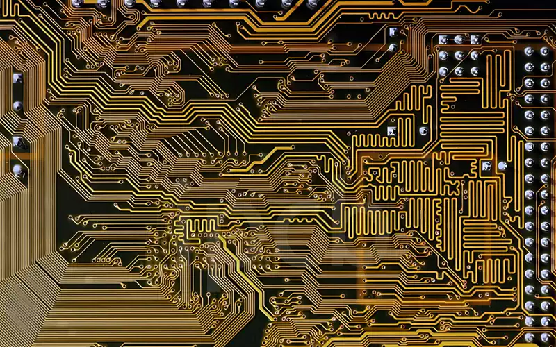
According to the level of holes through the PCB inner and outer layers, holes can be divided into through holes, buried holes and blind holes.
Through hole through the entire PCB, can be used to realize the inner layer of the connection and / or component positioning and installation. Among them, for component terminals (including pins and wires) and PCB fixed and / or realize the electrical connection of the hole is called component hole. Coated holes used for inner layer connection, but not inserting component leads or other reinforcing materials are called through holes. The purpose of drilling through holes in a PCB is twofold: first, to produce an opening through the board that allows subsequent processes to form electrical connections between the top, bottom, and inner layer wiring of the board; and second, to enable the mounting of components on the board to maintain structural integrity and positional accuracy.
Blind and buried vias are widely used in HDI for high density interconnects. blind vias typically connect layer 1 to layer 2. In some designs, blind vias can connect Layer 1 to Layer 3. Combining blind and buried vias allows for more connections and higher board densities required for HDI. This allows for increased layer density in a smaller pitch device while also increasing the power transferred. Hidden via holes help keep boards lightweight and compact. Blind and buried hole designs are common in complex, lightweight, and high-cost electronics such as cell phones, tablets, and medical devices.
Blind vias are formed by controlled drilling depth or laser ablation.The latter is the more common method used today.Stacking of via holes is formed by sequential lamination. The resulting via holes can be stacked or staggered,adding additional steps in manufacturing and testing, as well as increasing costs.
Countersink/Counterbore Hole: Also known as countersunk, stepped, funnel or flared holes.Typically used when the head of a flat head screw is required to be below the surface of the part. There is a flared opening on one or both sides of the board.The holes are tapered and move away from the center of the board as the diameter increases. This flared opening provides clearance for the head of a fastener such as a screw or bolt when fastened to the PCB board.
The role of countersunk holes:
Countersunk holes provide a tapered opening for fasteners and offer the following significant advantages:
Consistent Fastener Head Clearance:Ensures consistent clearance between the fastener head and pads or alignments on the PCB surface.
Flush Fastener Head:When using flat head screws, the countersink depth allows the fastener head to be flush with the PCB surface.
Smooth Surface Finish:Provides a continuous surface suitable for EMI shielding, gaskets and housings.
No Component Interference:Provides sufficient clearance between the electronic component and the fastener head for easy component placement.
Consistent Board Level Support:Countersunk hole edges provide consistent edge support to the PCB surface around the fastener.
Improved manufacturability:Simplifies the assembly process and allows for certain positioning tolerances.
Countersunk holes are mostly non-plated hole designs and are divided into two categories:
Tapered Countersink HoleCountersink Hole: Usually made so that the head of a countersink rivet, screw or bolt is flush or below the surface of the surrounding material.
Cylindrical Countersink HoleCounterbore Hole:A cylindrical and flat bottomed hole
The manufacture of countersunk head holes involves a number of processes, mainly consisting of the following steps:
Drilling: First, according to the design requirements, use a special drill bit to accurately drill holes in the PCB board. The holes formed at this time are straight and cylindrical, with the same caliber at the top and bottom.
Chemical copper deposition: Through electroplating or chemical deposition, the hole wall is covered with a thin layer of copper to realize the subsequent plating filling.
Orifice Chamfering:Mechanical or chemical methods are used to treat the orifice to give it an inward slant, i.e. to form a countersunk shape. This process requires precise control of the angle and depth to ensure that the hole is flat and meets the design requirements.
Plating and Filling:The hole that has been formed into a countersunk shape is plated and filled with copper or other metal material to make a well-conducted connection.
Surface treatment: Finally, conventional surface treatment steps such as soldermask coating and screen printing of characters are performed to complete the production of countersunk holes.
Through-hole
Through-hole (VIA) is a common hole used to conduct or connect the copper foil line between the circuit board layer and the conductive pattern in the layer. For example, holes, buried holes, but not copper-plated holes for inserting component leads or other reinforcement materials. Because the PCB circuit board is made of many layers of copper foil stacked cumulative, each layer of copper foil will be laid between a layer of insulation, so that the copper foil layers can not be interoperable with each other, the signal connection needs to be through-hole to achieve.
The characteristics of the guide hole is in order to meet customer demand, the circuit board guide hole must be plugged holes, so that in the change of the traditional aluminum sheet plug hole process, with white mesh to complete the circuit board board board blocking brilliant and plug holes, so that its production stability, reliable quality, and the use of a more perfect.
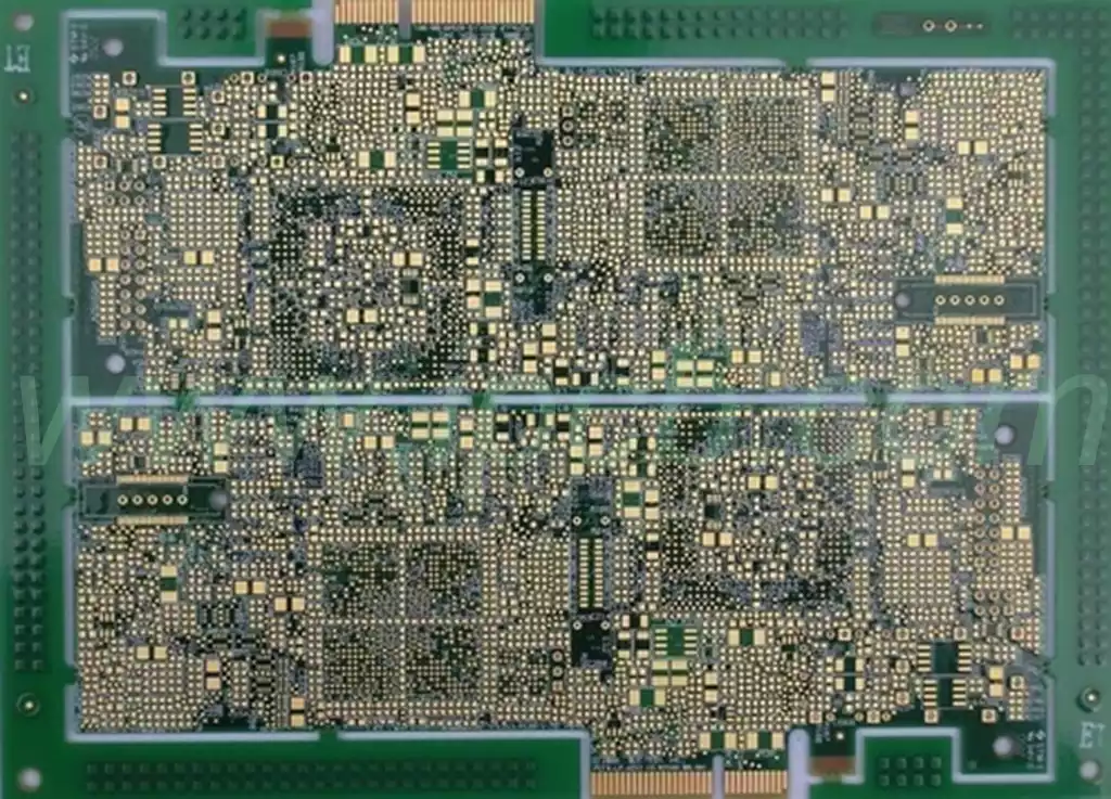
Circuit board has types of holes, from the basic plated holes and non-plated holes, to the complex through holes, blind holes and buried holes, each type with its unique features in electronic manufacturing play an irreplaceable role. These holes are not only the bridge for circuit connection, but also the key to realize high performance and reliability of electronic devices. As technology continues to advance, the design and manufacturing process of circuit board holes continues to innovate to meet the needs of increasingly complex and changing electronic products.