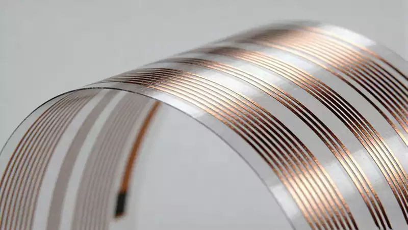
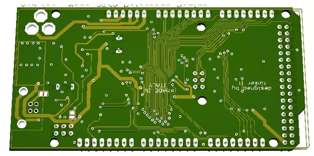
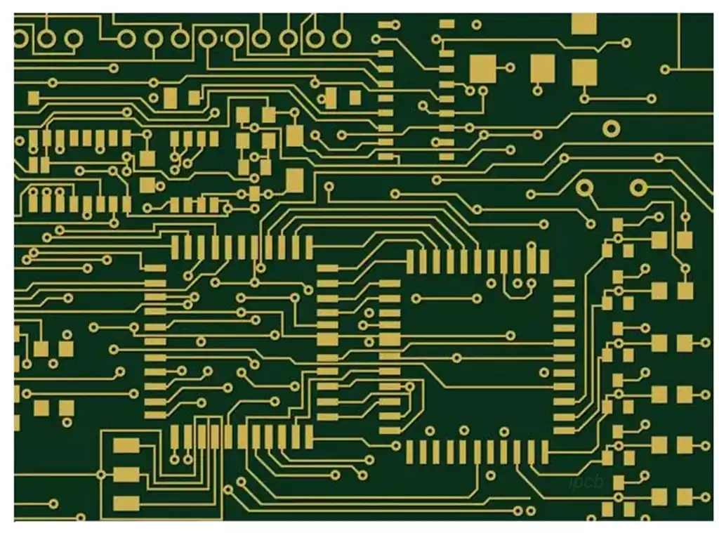
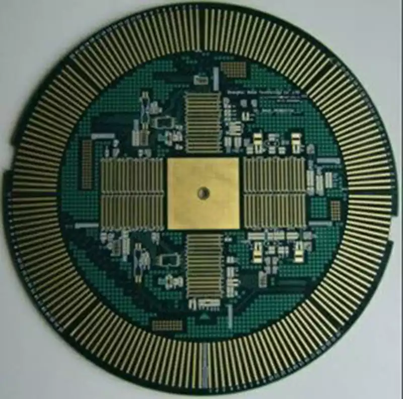
ABF substrates (Ajinomoto Build-Up Film) is a high-performance substrate for semiconductor packaging, known as “building block substrate”, which is mainly used in high computing performance chips such as CPUs, GPUs, FPGAs, and ASICs, and is popular for its high density, small size, and excellent heat dissipation characteristics. Popular for its high density, small size, and excellent heat dissipation characteristics, ABF substrates are able to directly form circuit lines by chemically plating copper without hot lamination through the use of layered thin-film materials.
The main features of ABF substrates include:
High-density wiring: ABF substrates enable fine lines and high-density wiring, which is suitable for high-performance chips.
Excellent electrical performance: low dielectric constant and dielectric loss, suitable for high-speed signal transmission.
Good thermal performance: ABF substrate material has good thermal conductivity and thermal stability, which helps chip heat dissipation.
High reliability: ABF substrate has good mechanical and environmental adaptability, which can ensure the long-term stable operation of the chip.
The core structure of ABF substrate usually retains the glass fiber cloth prepreg resin (FR-5 or BT resin) as the core layer, and at the same time, it adopts the design of incremental layer to build the substrate by using the ABF laminated dielectric film.
The incremental layer structure it employs can significantly increase its multilayer count and line fineness,making it more suitable for the needs of high-performance computing chips. The structure is designed to effectively meet the number of I/O ports of complex chips.
Manufacturing process of abf substrate
Core board production
The manufacturing process for ABF substrates begins with the fabrication of the core board. This stage typically includes material opening, drilling, and line etching, in addition to automated optical inspection (AOI) to ensure quality.
Lamination
After the core board is fabricated, ABF lamination is performed on the top and bottom of the core board.This process involves overlaying the ABF film on the surface of the core board and laser drilling to create microvias for subsequent metallization.
Plating and Patterning
Next, after completing the metallization of the holes, a series of dry film attachment, exposure, development, and pattern plating steps are performed. These processes are used to form the desired circuit pattern and ensure electrical connectivity of the circuit.
Circuit Constant and Baking
After circuit patterning is complete, technicians also perform curing, cleaning, and baking to ensure the stability and reliability of the pcb substrate. These steps are critical to maintain the overall performance of the substrate and further improve production yields.
Final Inspection and Quality Control
After all production processes are complete, ABF substrates undergo a rigorous quality inspection. This includes testing for line integrity, dimensional accuracy, and thermal performance to ensure that the final product meets industry standards.
Main application areas for ABF substrates
- High performance computing chips
ABF substrates are widely used in high-performance computing chips, especially in central processing units (CPUs) and graphics processing units (GPUs). These areas place high demands on the substrate, and ABF materials are able to support finer lines and higher pin counts to meet the complexity and precision of modern computing needs. - FPGAs and ASICs
In addition to CPUs and GPUs, ABF substrates are also suitable for Field Programmable Gate Arrays (FPGAs) and Application Specific Integrated Circuits (ASICs). The high insulation and excellent thermal properties of these substrates make them excellent for these applications, especially in scenarios that require flexibility and high performance.
Communications and 5G Base Stations
There are also important applications in communications technology, especially in 5G base stations. With the popularity of 5G networks, there is an increasing demand for high-performance and low-power substrates, and it is well positioned to meet these requirements.
Artificial Intelligence and Machine Learning
The demand for ABF substrates has risen with the booming development of artificial intelligence and machine learning. ai chips usually require high computing power, and high-quality substrates can provide good support to facilitate the efficient operation of ai related applications.
Server and Data Center
The application of ABF substrates is also becoming more common in the server and data center sectors. Due to the urgent need for high bandwidth and low latency, the performance characteristics of this substrate make it an important material to support the computing power of modern data centers.
Key Quality Control Measures in ABF Substrate Production Process.
1.Automatic Optical Inspection (AOI)
Automatic Optical Inspection (AOI) is one of the key quality control measures during the production process. This technology is used to perform quality checks after line etching at the core board production stage to ensure the integrity and accuracy of the line, thereby reducing the risk of errors in subsequent processes.
- In-process quality control
Each part of the production process requires strict quality control. For example, in the plating and patterning process, each step of the process must be tested to confirm that the resulting circuit pattern meets the requirements. This real-time quality control can detect problems and make adjustments in a timely manner, effectively improving inspection efficiency. - Curing, cleaning and baking
After completing the circuit pattern, curing, cleaning and baking are critical steps to ensure the stability and reliability of the substrate. These processes can eliminate impurities and unstable factors that may arise during the production process to ensure the performance and reliability of the final product.
4.Final Inspection
In the final stage of production, a comprehensive final inspection is performed. This step often includes systematic testing of line integrity, dimensional accuracy, heat resistance, and other aspects to ensure that the final product meets industry standards.
- Material and Process Standards
Ensuring that the raw materials used and the production process comply with the relevant standards is also another important quality control measure. In the production of ABF substrates, the quality of ABF films, coatings and other chemical materials used directly affects the performance of the final substrate, so the quality of these materials must be reviewed and verified on a regular basis.
Differences between BT encapsulated substrates, ABF encapsulated substrates and MIS encapsulated substrates
- The full name of BT resin is “Bismaleimide Triazine Resin” developed by Mitsubishi Gas Corporation in Japan. Although the patent period of BT resin has expired, Mitsubishi Gas Corporation is still the world leader in the development and application of BT resin, which is characterized by high Tg, high heat and humidity resistance, low dielectric constant (Dk), low dielectric constant (Dk), and high temperature and humidity resistance. dielectric constant (Dk), low dielectric constant (Df) and many other advantages. However, due to the presence of the glass fiber layer, it is stiffer than the FC substrate made of ABF. Although the alignment is more cumbersome and laser drilling is more difficult to meet the requirements of fine lines, it can stabilize the size and prevent thermal expansion and contraction from affecting the line yield, so it is mainly used in BT materials. High reliability requirements of network chips and programmable logic chips.
2.ABF material is a material dominated by Intel, used in the production of flip chip and other high-end carrier substrate, high dielectric constant soft substrate, mainly used for high mixed-signal, multi-layer high-density packaging.ABF material than the BT substrate can be made to the circuit thinner IC, the number of pins, the transmission rate is high, mainly used in the CPU, GPU, chipset, and other large-scale high-end chips.ABF is a laminated material that can be used as a circuit by directly attaching ABF to a copper foil substrate and does not require a hot crimping process. Developed by Japan’s Ajinomoto and monopolizing the source of the material, ABF is known for its important characteristics such as high durability, low expansion, and ease of processing.
- MIS substrate packaging technology is a new and rapidly growing technology in the analog, power IC, and digital currency markets. the difference between MIS and traditional substrates is that it contains one or more layers of pre-packaged structures, each interconnected with electroplated copper to provide electrical connections during the packaging process.
ABF substrates are becoming an important material for the semiconductor packaging industry due to their high density, small size, and excellent heat dissipation characteristics. Demand for ABF substrates will continue to grow with the rapid development of high-performance computing, artificial intelligence, and 5G technologies.
