In the electronics industry, pcb plays a vital role. It is the support of electronic devices and the key to circuit connection. In the development history of pcb, multi-layer pcb has been widely used, while 3 layer pcb is relatively rare in actual circuit board processing due to its unique structure and performance.
Why are three-layer circuit boards rarely seen in the pcb processing industry? With the continuous development of science and technology, the previously common single-sided and double-sided circuit boards have now developed to four, six or more layers. Has anyone ever wondered why there are no three-layer circuit boards in the pcb processing industry? The answer is yes. 3 layer pcb are relatively rare. Three-layer circuit boards have one more copper foil and bonding layer than four-layer circuit boards, and the cost difference is not much. That is to say, the price of your three-layer circuit board design is the same as the price of your four-layer circuit board design.
- The same processing process
The manufacturing process of three-layer circuit boards and four-layer circuit boards in pcb factories is the same. Usually, a copper foil is pressed on both sides of the core of a four-layer circuit board, and a copper foil is pressed on one side of the core of a three-layer circuit board. In terms of the process flow, it is necessary to stamp. - The same price
The difference in the cost of the two processes is that the four-layer circuit board has an extra layer of copper foil and bonding layer, and the cost difference is not much. When pcb manufacturers quote, they usually quote 3-4 layers as a level, and the quotation is defined by an even number (of course, more than multiple layers). For example, if you design a five-layer circuit board, the other party will quote according to the price of a six-layer circuit board, that is, the price of the three-layer circuit board you designed is the same as the price of the four-layer board you designed. - Process stability
In the pcb processing technology, four-layer circuit boards are easier to control than three-layer circuit boards. Mainly in terms of symmetry, the warpage of four-layer circuit boards can be controlled below 0.7% (IPC600 standard). However, when the size of the three-layer circuit board is larger, the warpage will exceed this standard, which will affect the reliability of the SMT patch and the entire product. Therefore, electronic designers do not design odd-layer circuit boards. Even if the odd-numbered layers realize the function, they will be designed as pseudo-even layers, that is, 3 layers are designed as 4 layers, and 5 layers are designed as 6 layers.
Structural characteristics of 3 layer pcbs
Compared with single-layer pcbs and double-layer pcbs, three-layer pcbs have a richer hierarchical structure. It consists of two inner copper layers and one outer copper layer, and the inner copper layers are connected through vias to form circuit connections.
Three-layer pcbs also have better thermal conductivity and electromagnetic shielding performance, and can provide better solutions under complex circuit wiring requirements.
The manufacturing process of three-layer pcbs is complex
Compared with single-layer pcbs and double-layer pcbs, three-layer pcbs require more processes and more complex processes in the manufacturing process. First, the manufacturing of the inner copper layer requires complex exposure and etching processes, and the circuit connection between the inner copper layers requires the use of precise hole plate design and technology.
Secondly, in the process of multi-layer stacking, interlayer bonding and lamination are required, which requires manufacturers to master higher process levels and precise equipment.
The cost of three-layer pcbs is relatively high
Because the manufacturing process of three-layer pcbs is relatively complex and requires more processes and equipment, its manufacturing cost is relatively high. In the context of fierce competition in the electronic product market, cost control is one of the important considerations for enterprises. Compared with three-layer pcbs, single-layer pcbs and double-layer pcbs are more economical and affordable, and can also meet the needs of most products.
Another reason why 3 layer pcbs are less visible in circuit board processing is the limitations of market demand and application scenarios. Although 3-layer pcbs have their application advantages in certain specific fields and products, such as high-frequency signal transmission, high-density integrated circuits, etc., in general, single-layer pcbs and double-layer pcbs can meet the wiring needs of most electronic products.
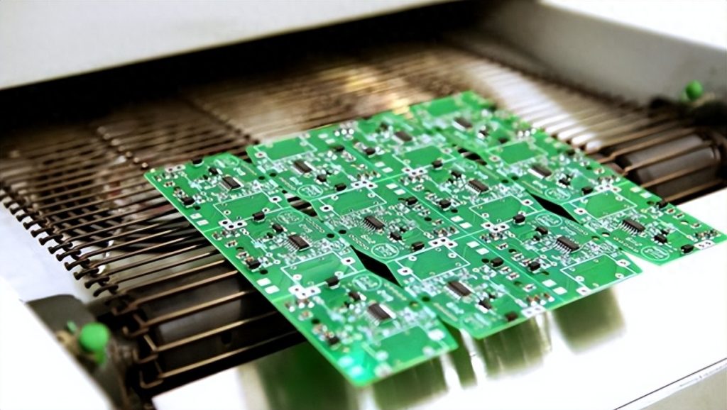
In the face of a market environment with high demand and short cycles, manufacturers are more likely to choose simpler and faster pcb structures to meet customer needs. Therefore, driven by commercial interests, manufacturers are more inclined to choose lower-cost pcb structures.
Detailed explanation of the production process of multi-layer pcbs
- Pre-treatment and pattern transfer
The first step in pcb production is to prepare the substrate-copper clad laminate. This step includes thorough cleaning, degreasing, and possible micro-etching to ensure the cleanliness of the copper clad laminate surface and good adhesion in subsequent processes. Then, through photolithography technology (or pattern transfer technology), the pre-designed circuit pattern is accurately transferred to the copper clad laminate and covered with a layer of anti-etching layer. This anti-etching layer will protect the copper layer that does not need to be etched and is the basis for realizing the circuit pattern. This step is a key link in pcb production and lays the foundation for subsequent processes.
- Etching and hole-forming
Chemical etching or laser etching technology is used to remove the copper foil not covered by the anti-corrosion layer to form a circuit pattern. Subsequently, holes are drilled at designated locations, which will be used for interlayer connections, such as PTH (plated through hole) or microvias. The hole-forming process is to form a conductive layer on the hole wall by chemical or laser technology to prepare for subsequent electroplating. - Lamination and interlayer connection
The characteristics of multilayer pcb boards are the stacking and connection of multilayer circuits inside them. By placing dielectric materials (such as epoxy resin) between pre-treated circuit layers and laminating them under high temperature and high pressure, an integrated multilayer structure is formed. Then, electrical connections between layers are achieved by electroplating through holes or microvia technology. - Surface treatment and inspection
In order to protect the circuit from oxidation and corrosion, the circuit board needs to be surface treated. Common ones include HASL (hot air leveling), ENIG (chemical nickel gold), OSP (organic solder preservative), etc. After that, the circuit board is fully checked for quality by means of automatic optical inspection (AOI), X-ray inspection, etc. to ensure that there are no open circuits, short circuits or bad connections. - Cutting and finished product testing
The large board is divided into individual circuit boards using mechanical punching or laser cutting technology. After cutting, each circuit board is also subject to functional testing to verify whether its electrical performance meets the design requirements. The qualified circuit boards will be cleaned, packaged, and ready for delivery to customers.
The production process of multi-layer pcb boards, from substrate preparation to finished product testing, embodies the art and science of precision manufacturing in every step. The foundation is laid by pre-processing and graphic transfer, the circuit is shaped by etching and perforation, and the multi-layer integration is achieved through lamination and interlayer connection, supplemented by surface treatment and strict inspection to ensure quality until cutting and finished product testing are completed. This series of complex and delicate processes together create the stable quality of multi-layer pcb boards and provide a solid foundation for the innovative development of the electronics industry.
There are many factors to consider. If you are not familiar with multi-layer pcb design, you may wonder what the most important issues are when designing circuit boards. From the number of layers to wiring and alignment to the overall layout. If you have any doubts, consider hiring a professional. Listed below are some of the most important questions to ask your clients when designing multi-layer pcbs.
What are the advantages of 3 layer pcbs? In short, multi-layer pcbs are more complex than single-sided pcbs because they have more layers and space, they can handle more circuits and add more features. Multi-layer pcbs are ideal for high-end devices such as smartphones. These boards can perform many of the same functions as multiple single-sided boards.
The different layers of a 3-layer pcb have different layouts and bottom materials. Routing is on the bottom and top layers of a 2-layer pcb, and each layer of a 4-layer pcb is connected to the next layer through a solid copper layer. The layout of these layers is critical to the success of your product, and a custom pcb design file should clearly define all the planes that will be used. In addition to layout and routing, t3 layer pcbs also have a wider variety of components.
The materials and properties of the layers used to create a 3-layer pcb vary. For example, one type has a metal core, while another is insulated with a conductive material. A special adhesive bonds the layers together. The insulating material protects the outer layers. Each layer is also separated by a conductive material. The board is usually multi-layered.
To sum up, the reason why 3 layer pcbs are less visible in circuit board processing is mainly due to the complexity of its manufacturing process, high cost, and limitations of market demand and application scenarios. Although it has certain advantages and characteristics, it is still subject to various restrictions in practical applications. As a pcb/pcbA manufacturer, we can make 3-layer pcbs without any problems, even if it is a unique product. We are very good at custom products.
In fact, we have made many special and unique pcbs for leading brands in the electronics industry.
We are usually the first choice for OEM or EDM pcbs, not only for 3 layer pcbs, but also for RF pcbs, SSD pcbs, drone pcbs, etc. If you want to learn more, please contact us now!
