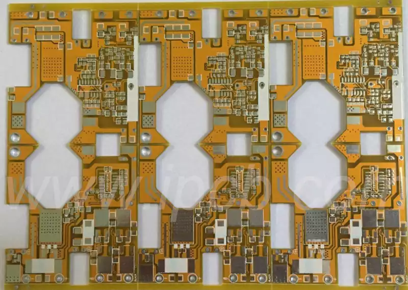
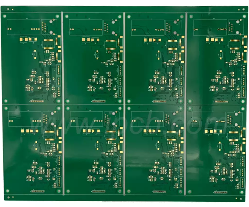
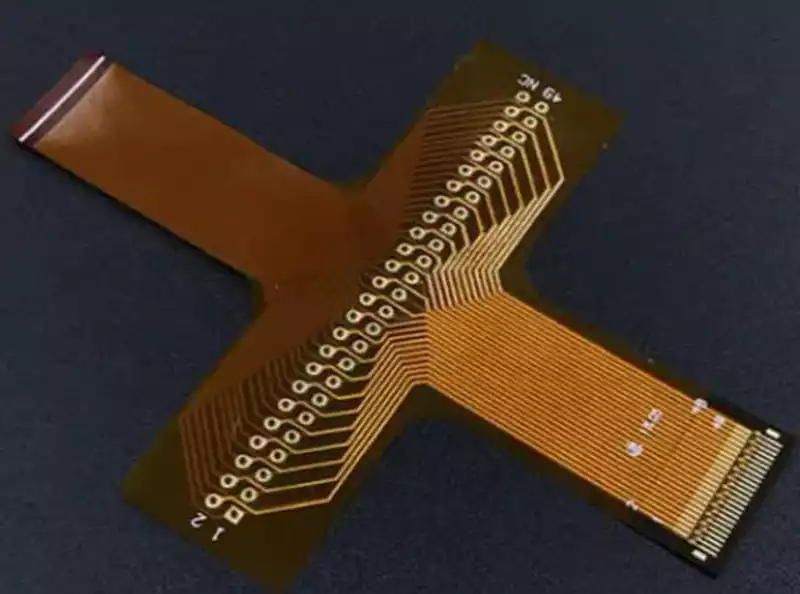
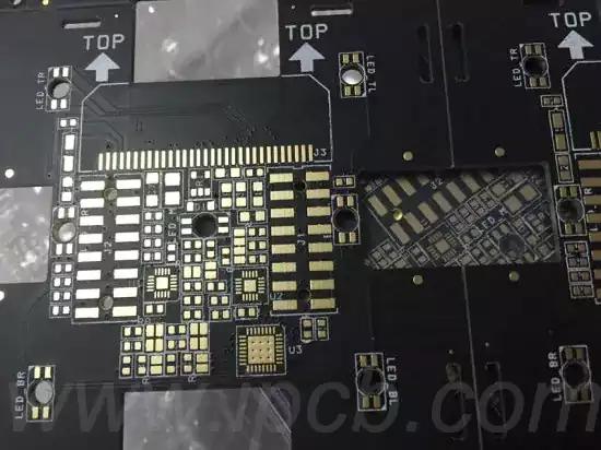
Insulate Metal Substrate, as a type of computer motherboard, aims to improve thermal efficiency and mechanical strength by applying metallisation to a thick substrate. It is also known as aluminium substrate, aluminium cladding or metal clad PCB (MC PCB), and even thermally conductive PCB (in fact, all PCBs are thermally conductive). Compared to the regular models of the R4 and R3, the thermal performance can be increased by a factor of three to ten. Highlighted on the side of the lens is the Metallised Platelet PCB (MSPCB), which is mounted on top of the aluminium.
In this insulate metal substrate PCB (IMS PCB), the metal surface is covered with an insulating coating. Thus, IMS PCBs incorporate metallic materials, either in thin or embedded layers, to enhance the mechanical strength and thermal conductivity of the board. In addition, this type of PCB is widely recognised for its use of metal core components and aluminium coatings. Traditional standard printed circuit boards (PCBs) can be effectively replaced by a high-quality alternative in the form of PCBs with metal cores. These components are particularly suitable when circuits require high-density stability or must be kept away from the high temperatures generated by LEDs and power supply components.IMS boards are constructed from aluminium and exhibit excellent thermal conductivity, making IMS-compatible PCBs an even more reliable choice for devices.
Single-sided Insulate metal substrate PCB
The basic components of a single-sided insulate Metal substrate pcb consist of a sheet of copper foil, which is adhered to a thermally conductive material and bonded to a metal substrate.Generally, PCB manufacturers are able to source copper clad laminates from a wide range of laminates manufacturers that have been laminated to a metal substrate. When designing a single-sided IMP PCB, the following key elements need to be taken into consideration.
The standard thickness range of copper layers is usually between 1 oz and 6 oz, while the most common copper thicknesses are 1 oz to 2 oz.An increase in copper thickness results in higher PCB production costs.
The thermally conductive semi-cured sheet is a crucial element in this construction and its properties will vary depending on the supplier.It acts as an insulating material that separates the electrically conductive copper circuitry from the main metal substrate while effectively facilitating rapid heat transfer between the two. This property ensures that the heat generated by the device is quickly dispersed to the metal substrate (i.e. heat sink).
Semi-cured sheets are usually composed of organic resins with ceramic fillers that enhance their thermal conductivity. The type, size and form of the ceramic filler, as well as its proportion in the resin, are key factors in determining its thermal conductivity.Common ceramic fillers include aluminium oxide (Al2O3), aluminium nitride (AlN) and boron nitride (BN). Thermal conductivity can be assessed by thermal conductivity (in Watts per metre Kelvin, or W/mK) and thermal impedance (in Kelvin square metres per Watt, or Km²/W).Higher thermal conductivity indicates better heat transfer efficiency, while lower thermal impedance likewise implies better heat transfer performance.
It is important to note that the increase in thermal conductivity of semi-cured sheets is often accompanied by an increase in cost, so it is important to avoid over-design. A good judgement is required, as FR-4 thermally conductive substrates have a thermal conductivity of around 0.4 W/m-K, while common commercially available thermally conductive semi-cured wafers have a thermal conductivity of between 1 W/m-K and 7 W/m-K. In addition to the thermal conductivity, the thickness of the dielectric layer is also a key factor, with a common range of 2 mils to 6 mils.
Aluminium is the material of choice for metal substrates. Of the base metals, 5052H32 and 6061T6 are the two most common types, with 5052H32 generally being more economical and more commonly used than 6061T6. Aluminium thicknesses range from 40 mils to 120 mils, with 40 mil and 60 mil thicknesses being the most common. Copper is also chosen as the base metal in some application scenarios, but this is a relatively costly option.
The cost of insulate metal substrate laminate materials is significantly higher than FR-4, so it becomes especially important to make effective use of board/array design in the board manufacturing process. Co-design with the PCB manufacturer is critical. The most common size for this type of material is 18‘ x 24’.
Solder Resist
Single-sided insulate metal substrate pcb design is quite suitable for LED applications, but the key is to use white soldermask. Many LED customers are looking for uniformity in the colour of the soldermask, however, even the soldermask products on the market that are also labelled as LED-specific are not all the same colour.
Part of the soldermask is bluish, and part is yellowish. In addition, the colour of single layer soldermask and double layer soldermask also differ, which is another factor to be taken into account. At the same time, there is an interaction between the surface coating, the soldermask and the heat treatment step in the subsequent assembly process. Some soldermasks may change colour due to increased temperatures. Boards with lead-free hot air levelling (HASL) tend to be more susceptible to yellowing of the soldermask due to the higher heat exposure. Therefore, it is recommended that boards be allowed to pass through the Pb-free HASL process only once (i.e., to avoid rework in this process).
Processing and Manufacturing
V-cutting is the most common method used when machining square or rectangular plates.The advantage of V-cutting is that it maximises material utilisation as there is no spacing between the two parts after cutting. In contrast, milling is the most costly, as it is time consuming and requires spacing between the two parts, which can reduce material utilisation. Make sure that your PCB manufacturer has a V-cutting system designed for dividing aluminium substrates and that it is equipped with lubrication. Diamond coated cutting blades are recommended when working with aluminium based PCBs.

Double-sided/multilayer PCBs
PCB manufacturers first create double-sided or multi-layer insulate metal substrate PCB, which are subsequently laminated to a metal substrate by a multi-layer lamination process using thermally conductive semi-cured sheets.This lamination process is accomplished using a multilayer laminator.
Many of the same design considerations and caveats that apply to single-sided insulate metal substrate pcbs are also critical for double-sided insulate metal substrate pcbs.In addition, double-sided insulate metal substrate pcbs need to be designed with other specific factors in mind, including:
The increased weight of the copper layers can drive up costs, while the through-holes on the outer two layers also need to be plated, further increasing the amount of copper used. Wiring and wire spacing should be based on the copper weight of each layer and follow the design specifications provided by the PCB manufacturer.
Double Sided vs. Multilayer Construction Design
It is critical to decide whether to use FR-4 to build the multilayer board, or whether to require a thermally conductive semi-cured sheet with a core board.
If the latter is chosen, there are a number of options available, but there are limitations on the thickness of the core board, so it is best practice to discuss the core board structure with the PCB manufacturer or CCL supplier. Due to the low fluidity of semi-cured sheets, it is particularly important to communicate with the PCB manufacturer in advance to fully understand the lamination and press cycle used for these materials.
Selection of thermally conductive semi-cured materials
Depending on the thickness of the copper circuits and the required thermal conductivity, an appropriate semi-curing sheet needs to be selected to bond the PCB (whether double-sided or multi-layer) to the metal substrate. From the PCB manufacturing point of view, a number of factors need to be taken into account when pressing the PCB onto the metal substrate:
The need to ensure that there is no delamination between the PCB and the metal substrate. Design factors and process conditions during lamination can affect delamination;
The existence of a method to control the flow of semi-cured flakes through the plated through holes to the top, and a method to prevent the flow of semi-cured flakes to the surface of the PCB;
The existence of mismatches in the coefficients of thermal expansion (CTE) between constituent components, it is critical from the PCB’s point of view to try to balance the copper content of the structure and to ensure that the press-fit cycle helps to minimise warpage.
Metal Substrate Materials
Aluminium is the most commonly used metal substrate material, but copper is also used in many applications. Overall, aluminium is the best choice, with 6061T6 alloy being the optimum option for this structure.
Metal Core PCB Structures
Conceptually, a metal core PCB is, as the name suggests, a sheet of metal embedded in the dielectric layer of the PCB and located between several layers of circuitry. Metal core PCBs typically have blind vias on both sides of the metal core substrate and plated through holes (PTH) throughout the board. From a PCB perspective, it is critical to ensure that the metal remains isolated from the vias, otherwise the board will be completely shorted. To achieve this, holes are drilled or slotted into the metal core with diameters 40 mils to 50 mils larger than the plated-through holes, which are subsequently filled with a non-conductive epoxy filler and then press-fit. Upon completion of the press fit, the filler mixture is removed from the metal surface and the inner core is then prepared for press fit. At the end of the lamination, the PTH holes are drilled and processed according to the normal manufacturing process.
One of the reasons for using this type of PCB is its thermal performance, and another is that it helps reduce vibration, thus ensuring that components do not fall off the PCB in high vibration applications.
Design Considerations:
Core material/semi-curing medium
Core materials/semi-cured media are available in a variety of PCB base materials, including metal core boards made from polyimide, FR-4 or high thermal conductivity materials. The choice of material depends entirely on the electrical performance requirements or thermal management strategy.
Metal Core Material Selection
Metal cores are typically made of copper 110 or aluminium 6061T6. In metal core board applications, the number of copper and aluminium core designs is almost equal.
Metal Core Drilling Process
Whether it is a plated through-hole through the top to bottom layers or a non-plated through-hole, the diameter of the holes drilled in the metal core board needs to be larger than the hole pattern on the PCB. Occasionally, additional clearance may not be required for mounting or grounding holes on the metal core.
Insulation/Filler Materials
Insulation/filler material is used to isolate the PTH from the metal core and prevent short circuiting of the entire PCB. The filler material is initially applied to the surface and within the holes in powder form, and is subsequently laminated in a multi-layer laminator. This process is critical because there must be no voids in the filler material, otherwise when drilling through holes, chemicals could seep into the metal core and cause a short circuit. The surface of the metal core is then sandpapered to remove any excess filler material. The filler material is mainly made of ceramic mixed with epoxy resin.
Stacked Layer Structure
The laminated structure should be symmetrical, i.e. the number of layers at the top of the metal core is equal to the number of layers at the bottom. In addition, the copper weight between the layers should be as symmetrical as possible, similar to a normal multilayer PCB. Asymmetry can lead to serious warpage problems. Overall, conventional IPC warpage standards do not apply to this type of PCB.
Milling
Most metal core PCBs require various milling processes to expose the metal core layer.
Surface Preparation of Exposed Metal Core
It is recommended that a surface treatment be applied to the exposed metal core. For aluminium cores, a chromate conversion film is recommended; for copper cores, a nickel plating layer with a minimum thickness of 50 micro inches is recommended.
Insulate metal substrate PCBs have become an indispensable key component in modern electronic devices due to their excellent thermal performance and mechanical strength. Through the combination of careful design and advanced manufacturing technology, insulate metal substrate PCBs not only enhance the performance and reliability of products, but also promote the continuous progress and development of the electronics industry.


