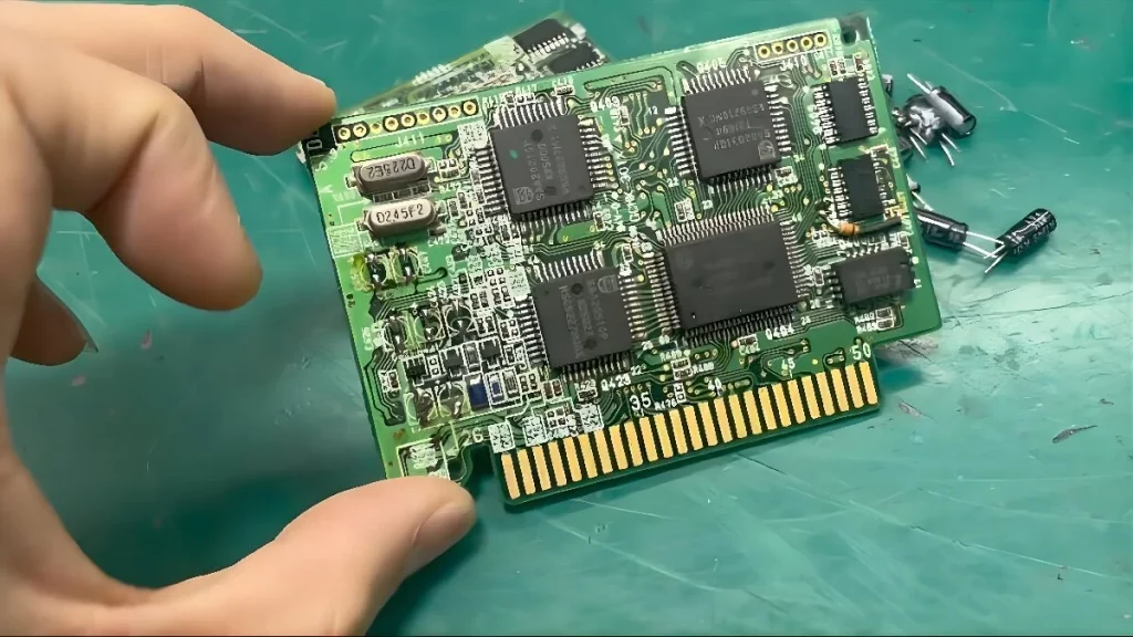
Circuit card assembly (CCA) is thin, flat board of dielectric material with conductive paths or tracks etched on their surface. In order to automate the production of CCAs, surface mount technology (SMT) and through-hole assembly machines are often used. Those responsible for the layout design and assembly of this form of manufacturing must have extensive professional experience. Similar to printed circuit board (PCB) assemblies, circuit card assemblies (CCAs) are used in a wide variety of household appliances, such as televisions, laptops, microwave ovens, smartphones, smoke alarms, and security cameras. They also play an important role in a variety of industries, including navigation systems, power supplies, automotive displays, medical imaging equipment, and monitors.
Different components of CCA
Circuit card assembly is a common feature of electronic devices. Even the most basic electronic products contain circuit components. The process of circuit card assembly involves connecting the wiring on the printed circuit board (PCB) to the electronic components. This assembly, also known as a printed circuit board assembly (PCBA), is constructed from the wiring in the copper PCB. Depending on the circumstances, these assemblies may be CCAs or PCBAs, but they are primarily composed of four key components. Therefore, it is especially important to have a basic knowledge of circuit assembly design. Regardless of the type of circuit board, they all contain the following basic components:
Substrate
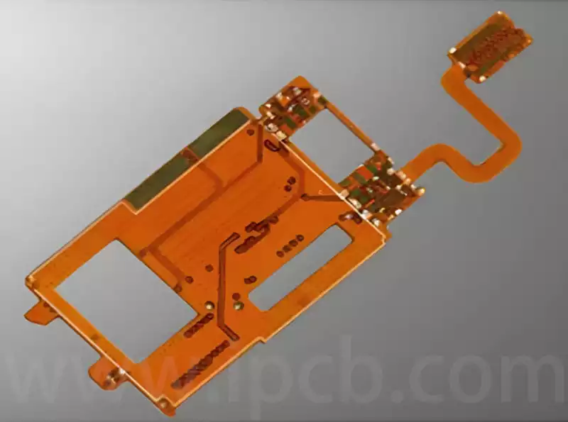
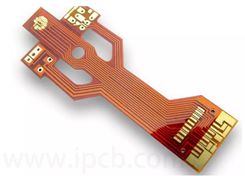
The infrastructure of a circuit card assembly is like a frame that holds all the electronic components securely in place. The sturdiness of a circuit board owes a lot to its substrate. Different types of PCBAs (Printed Circuit Board assembly) have their own distinctive substrates, such as soft ones, hard ones, and ones with built-in metal cores. Regardless of the type of board, the base layer, the ‘skeleton’, is mostly made of glass fibre. Of course, with the exception of flexible PCBs, which are particularly soft, most circuit boards use glass fibre as a base.
Copper
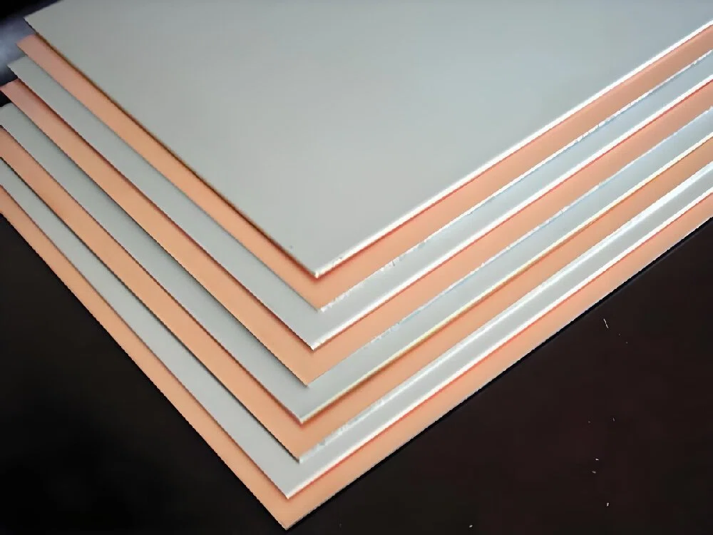
During the production of a printed circuit board, a thin layer of copper foil is added. The producer will use heat to press the CCA or PCBA substrate and the copper foil together tightly so that the electronic components can be connected by conductive lines or tracks. Different types of PCBs have different numbers of copper layers on them, with some having only one layer and others having several. For example, a single-sided PCB would only need copper foil on one side of the board.
Soldermask
Soldermask gives the board its trademark yellow or green colour. It’s actually a coating whose main purpose is to prevent the board from corroding and to reduce the risk of short-circuiting when soldering. Manufacturers apply soldermask to circuit boards, which encapsulates the copper layer and prevents other metals from coming into direct contact with the copper. With soldermask, the manufacturer has a better idea of where to solder when placing components.
Silkscreen
A silkscreen layer is usually added to the top and bottom of circuit boards. This layer is printed with symbols or descriptions that act as an ‘instruction manual’ for the circuit board so that engineers can understand it at a glance. These symbols, letters and numbers are printed on the board using a technique called screen printing. With these symbols, it is easier to figure out how the different LEDs and pins work.
Circuit Card Assembly Procedure
The circuit card assembly (CCA) assembly process is a multi-step process that involves applying solder paste to the circuit board, selecting and placing components, performing soldering operations, quality inspections, and performance tests, all of which must be strictly followed and effectively monitored in order to produce a quality product. All of these steps must be strictly followed and monitored in order to produce a quality product.The basic circuit card assembly process:
Step 1: Applying solder paste with the help of a stencil
In the CCA process, solder paste is first applied to the circuit board. In this step, the CCA manufacturer uses the solder paste to cover the circuitry on the board. The process is somewhat similar to screen printing on clothing, but instead of a mask, a thin stainless steel stencil is used to cover the PCB. solder paste, or solder as it is commonly referred to, is actually a grey substance made up of a myriad of tiny metal spheres, consisting mainly of 96.5% tin, 3% silver and 0.5% copper, and it is lead-free.
Flux is a key ingredient in solder paste and its role is to assist the solder to melt and adhere firmly to the surface. Manufacturers must ensure that the right amount of solder paste is applied in the right place. In order to accurately apply the solder paste to the intended location, a variety of application tools can be used. In a modern CCA production process, the PCB boards and soldering templates are held securely in place by mechanical equipment. The manufacturer then applies the solder paste in precise amounts to the designated areas. The machine then spreads the solder paste evenly over the stencil, ensuring that all blank areas are covered. When the stencil is removed, the solder paste stays securely in its preset position.
Step 2: Automated Component Placement
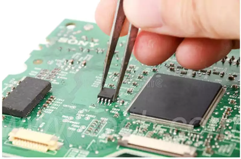
In this step of the assembly process, the boards, which have been coated with solder paste, move on to component pick and place. This step is done by automated machines. In this step, the manufacturer places a variety of SMDs (Surface Mounted Devices) and other electronic components exactly on the PCB. Nowadays, most of the components on a PCB are SMDs, except for the connectors, and then the CCA or PCBA process moves on to soldering these SMDs to the surface of the board. Component pickup and assembly of circuit boards can be done automatically or manually. Previously, assembly workers had to manually pick and place components one by one with tweezers to complete the job. Now, however, PCB manufacturers have automated this process.
At the heart of this change is the fact that machines typically have a higher degree of accuracy and reliability than humans. Whilst humans are able to complete tasks quickly, they tend to get tired and their eyes begin to strain after handling such tiny components for long periods of time. In contrast, a machine can run continuously without the slightest fatigue. the PCB is automatically transported by the machine to the pick-and-place station, where the machine initiates the pick-and-place process by utilising vacuum grippers to grip the PCB. The robot then positions the PCB precisely on the workstation and starts to apply SMT (surface mount technology components) to the surface of the PCB. These components are placed precisely on top of the previously applied solder paste.
Step 3: Reflow Soldering Process
Reflow soldering is the third stage after the component has been placed and solder paste has been applied. After the solder paste has been applied, the surface mount components need to remain in their original position. In order for these components to adhere firmly to the board, the solder paste needs to be hardened, and the circuit card assembly process achieves this through a process known as ‘reflow’. In the pick-and-place process, the PCBs are placed on a conveyor belt. This conveyor feeds the PCBs into a huge reflow oven, which in many ways resembles a commercial pizza oven. In this oven, which consists of multiple heaters, the boards are gradually heated up, eventually reaching a temperature of about 250 degrees Celsius (or 480 degrees Fahrenheit).
At this temperature, the solder in the solder paste will begin to melt. Once the solder is melted,the PCB continues to move through the oven. As the melted solder passes through a series of heaters at lower temperatures, it cools and solidifies in a controlled manner.In this way, a permanent connection is formed between the surface mounted component (SMD) and the PCB through the solder joint. Especially for those double-sided CCAs (Circuit Component Assemblies), there are several aspects of the reflow process that require special attention. Each side of a double-sided CCA requires separate stencil printing and reflow soldering. Typically, the side with the least amount of debris and smallest pieces will be stenciled, components placed,and reflow soldered before the other side.
Step 4: Testing and Quality Control
After the components have been placed correctly, the completed circuit component assembly as well as the assembled board need to be tested for functionality and assembly capability. During the reflow soldering process, movement can lead to connection failures or substandard connection quality. This movement also often leads to problems with missing components, as misplaced parts may be incorrectly connected to circuit segments that should not be connected, thus causing failures. In order to detect and correct these defects,we need to carry out an inspection.In this segment,we can choose between automated inspection or manual inspection.
In order to find these errors and displacements, we can use one of many different inspection techniques. Some of the most popular inspection techniques include X-ray inspection, manual inspection and automated optical inspection. When dealing with high volume circuit card assembly, automated optical inspection is the preferred choice. The equipment used for this technique is called an Automated Optical Inspection (AOI) machine, which is equipped with multiple high-performance cameras to ‘inspect’ the PCB. These cameras are set up in a number of different configurations in order to get a clear view of the soldered connections, and the AOI technology is able to identify poor quality solder joints, as different types of solder joints appear to reflect light in different ways. With their ultra-fast processing speeds, AOI machines are able to inspect large numbers of PCBs in a fraction of the time.
Despite the growing trend towards automated manufacturing, manual inspection is still an important method that the CCA industry relies on when dealing with small batches of CCA (circuit component assembly). This requires manufacturers to perform on-site manual visual inspections at the end of the reflow soldering process. This is an effective means of ensuring board quality. However, as the number of boards to be inspected continues to increase, this method of inspection becomes inefficient and less reliable. Long periods of time (more than an hour) spent looking at such tiny components can easily lead to eyestrain, which in turn affects the accuracy of the inspection. X-ray inspection is a different inspection technique.
This lesser-used inspection method is usually applied to more complex circuit boards or multilayers. With X-ray technology, the inspector is able to look through the layers and clearly see the lower layers in order to detect any potential problems. These inspections are often carried out at regular intervals after the reflow soldering process has been completed to search for any potential problems. By conducting such regular inspections, it ensures that problems are identified and resolved in a timely manner, thus saving the manufacturer time, labour and resources.
Step 5: Inserting through-hole components
The construction of a circuit board may vary depending on the type, and in addition to common surface mounted components (SMDs), boards under PCBA (Printed Circuit Board Assembly) may also contain other components. One example is plated through-hole components (PTH components for short). Plated through-holes are holes in a PCB that are fully plated and are designed to allow PCB components to pass signals from one side of the board to the other. In this case, solder paste is not useful, as it will pass right through the holes and not adhere. In subsequent stages of PCB assembly, PTH components require more specialised soldering processes. For example, in a simple manual soldering process, each component must be manually inserted into the corresponding PTH hole by staff at a single station.
Step 6: Final Inspection and Functional Verification
The final and crucial stage in the circuit card assembly process is verification, which is a direct reflection of the success of the entire process. Just as the reason for such testing, the inspections performed periodically throughout the assembly process are of equal importance to the testing. Once the soldering part of the PCBA process has been completed, the next final inspection focuses on the functionality of the PCB, which is known as ‘functional verification’. This verification tests the PCB by simulating its normal operating conditions. During the test, the PCB is plugged into a power supply and exposed to simulated signals, while testers closely monitor its electrical performance.
The manufacturing process for circuit card assembly is a systematic project that combines high technology with precision craftsmanship. From the precise application of solder paste, to the efficient placement of automated components, to the rigorous control of reflow soldering, each step is indispensable, and together they form the cornerstone of high-quality CCA production. Meanwhile, with the continuous advancement of automation and intelligent technology, CCA’s manufacturing efficiency and quality continue to improve.
