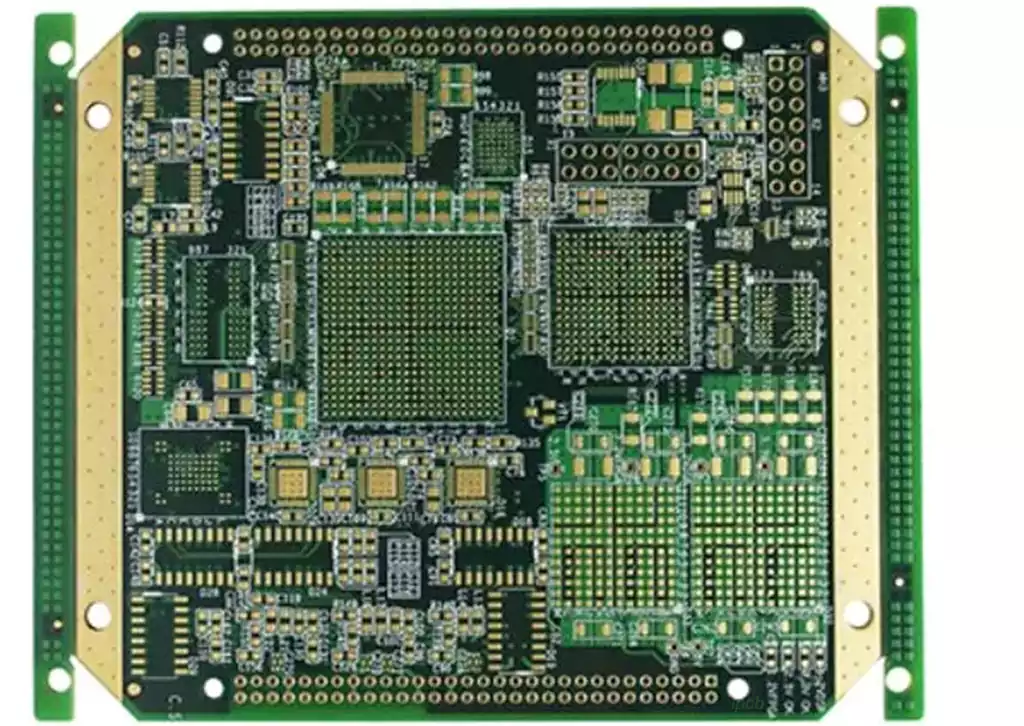
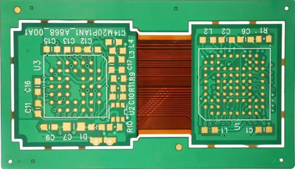
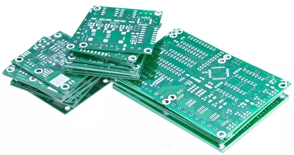
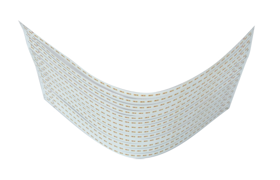
The stacked construction technique of HDI circuit boards allows multiple circuit layers to be interconnected by means of precisely tuned blind and buried vias, which are significantly smaller in diameter than the through-holes found in conventional PCBs. This fine interconnect mechanism not only reduces board size, but also significantly increases routing density, allowing more electronic components to be integrated in a limited space.
In addition, HDI’s stacked construction technology optimises the signal path. Signal delays and losses are effectively managed thanks to shorter distances and the avoidance of unnecessary twists and turns. This is critical for electronic devices seeking high-speed data processing capabilities, which need to respond quickly and accurately to the demands of processing large amounts of data.
HDI’s stack construction technology comes with its own set of challenges in the manufacturing process. To achieve high-precision processing of blind and buried vias and precise alignment of layers, manufacturers rely on sophisticated laser drilling technology and high-precision etching equipment. At the same time, the materials and processes used must be subjected to rigorous testing and validation procedures in order to guarantee the reliability and stability of the boards.
The raw materials required for manufacturing High Density Interconnect (HDI circuit boards) include the following categories:
- Substrate Material:As the main structure of the hdi circuit board, the substrate is usually composed of insulating materials such as FR-4 (i.e. epoxy glass fibre cloth), CEM series (epoxy glass fibre paper matrix composites), PTFE (polytetrafluoroethylene) and PI (polyimide). In order to achieve higher wiring density, HDI PCB may choose thinner substrate materials.
- Conductive medium:Copper is the main material for the conductive lines in the PCB and is responsible for building the conductive path of the circuit. Copper foil is often laminated to the substrate by electrolytic deposition or calendering.
- Isolation layer material:In the multi-layer HDI circuit board structure, the isolation layer plays the role of separating different conductive layers. Common isolation materials are epoxy resin, polyimide and so on.
- Adhesive media:Used to tightly combine the various layers of materials to ensure that the structure of the PCB is solid. Adhesives need to have good adhesion and electrical insulation properties.
- Microporous insulating coating:HDI circuit board using microporous technology to achieve a close connection between the layers, and microporous insulating coating is used to fill these microporous to ensure the reliability of the electrical connection.
- Surface protection materials: The surface treatment of HDI circuit board involves a variety of protective materials, such as hot air levelling (HASL), electroless nickel/impregnated gold (ENIG), electroless nickel/impregnated silver (ENS), impregnated tin (IT), and organic solderability protection (OSP) coatings, etc., which are designed to protect the copper surfaces and enhance soldering results.
- Solder Resist Ink: Solder Resist is used to cover areas that do not need to be soldered and to prevent short circuits during soldering. It usually consists of a photosensitive polymer and is patterned by photolithography.
- Marking ink: Used to mark component position, direction and other information on the PCB for easy identification by automated assembly equipment. Marking ink can be photosensitive or other types.
- Solder flux additives: used in the soldering process to help solder better wetting pads to improve soldering quality.
- Soldering Alloy: Alloy mainly composed of tin, lead, silver and other metal elements, used to connect electronic components with PCB.
- Cleaning solvents: In the manufacturing process, cleaning solvents are used to remove oil, fingerprints and other impurities on the surface of the PCB to ensure the cleanliness of the production environment.
- Other auxiliary tools and materials: including drills and milling cutters for PCB machining, as well as auxiliary materials for testing and inspection.
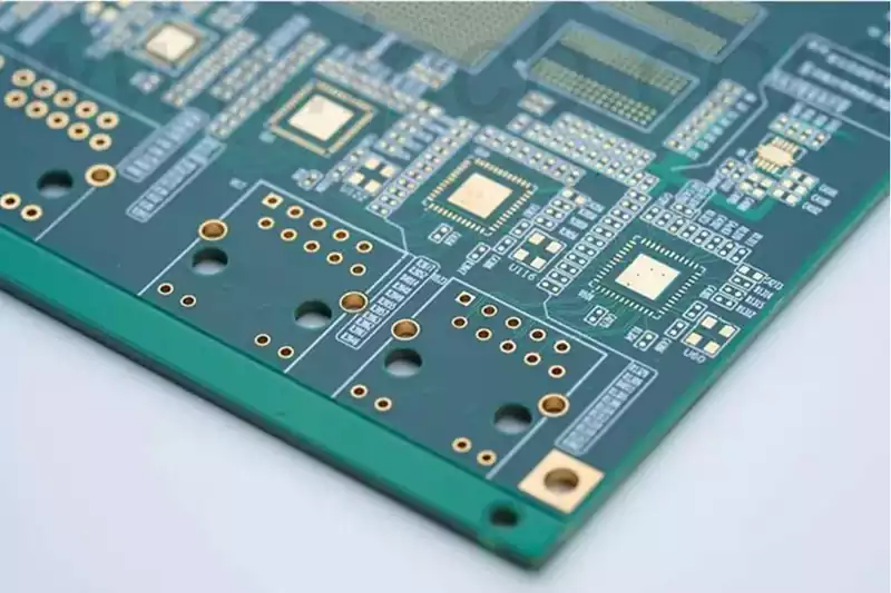
In high frequency signal transmission, in order to reduce energy loss, hdi circuit board materials need to have a low dielectric loss angle tangent (or dissipation factor Df) and a smoother Df curve for frequency response. For HDI applications, there are four categories of materials to choose from and they are:
Standard speed, higher loss
These materials are the most common in PCB manufacturing, such as the FR-4 series. They do not have a smooth enough curve of dielectric constant (Dk) with frequency and have relatively high dielectric loss. Therefore, these materials are mainly suitable for digital/analogue applications up to a few GHz. Isola 370HR, for example, belongs to this category.
Medium speed, medium loss
Medium-speed materials exhibit a smoother Dk versus frequency response curve and have about half the dielectric loss of standard-speed materials. These materials are suitable for applications up to about 10 GHz. the Nelco N7000-2 HT is an example of a material in this category.
High Speed, Low Loss
These materials not only have a smooth Dk vs. frequency response curve, but also have very low dielectric losses. They also generate less unwanted electrical noise than other materials, and Isola I-Speed is an example of a high-speed, low-loss material.
Very High Speed, Very Low Loss (RF/Microwave Applications)
Materials designed for RF/microwave applications with the smoothest Dk to frequency response and the lowest dielectric loss. These materials are suitable for applications up to approximately 20 GHz. isola Tachyon 100G is a prime example of this type of material. To improve signal transmission performance in high-speed digital applications, materials with lower Dk and Df and better SI characteristics should be used. For RF and microwave applications, materials with the lowest possible Df should be selected. When signal attenuation is a critical factor, low-loss, high-speed materials are the best choice. If phase noise is an issue, its effect can be reduced by using materials with lower Dk. BT materials are more appropriate when dealing with microelectronic substrates with small dimensions and compact layout features.
Challenges in the production process of HDI circuit board and conventional boards
The difficulties in the production of HDI circuit boards and conventional boards are mainly focused on design conception, material selection, process and testing, etc. The first is that at the material level, the structure of HDI boards is more complicated than conventional boards. First and foremost, at the material level, the structure of HDI boards is more complex than that of conventional boards, so the performance standards for the materials used are more stringent. For example, it may need to introduce some processing difficulty of the material, such as PTFE, PPO, PI, etc., these materials in the processing process is prone to thermal stress, dimensional changes and other issues, thus enhancing the difficulty factor of the production.
Secondly, in the interlayer interconnection, in view of the HDI circuit board design of the line in a large number of layers and connection points are dense, if the use of perforated connections, will lead to a steep increase in the frequency of perforation, which threatens the stability of the line and the overall performance of the board. Therefore, it is necessary to resort to blind and buried vias. However, both technologies involve a certain degree of difficulty and testing. Buried hole technology is difficult and costly; while blind hole technology depends on laser drilling, fixed depth drilling and other high-precision equipment support, but also may encounter the problem of substandard perforation quality.
Furthermore, the manufacturing process of HDI circuit boards is also complex. Layer method, for example, the increase in the number of layers means that the technical requirements of the enhancement. Ordinary HDI circuit boards more than 1 time layer, while high-level HDI may use 2 or more times the layer technology, and the simultaneous introduction of stacked holes, plating to fill the holes, laser direct punching and other cutting-edge PCB technology. Finally, the challenges of the HDI circuit board process also covers the control of PCB alignment accuracy, dimensional changes and compression process flow control and laser drilling laser energy regulation. All of these factors have the potential to have a profound impact on product quality and performance. Overall, HDI circuit boards are far more difficult to produce than traditional PCBs, and require deeper expertise and technical strength to guarantee product quality and performance.
HDI circuit board technology is revolutionising the electronics industry with its outstanding performance, and despite the many challenges it faces, manufacturers are continuing to improve the quality and performance of HDI boards through continuous innovation and technology optimisation, ensuring that they will be widely used in the electronic devices of the future.
