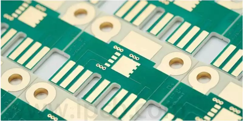
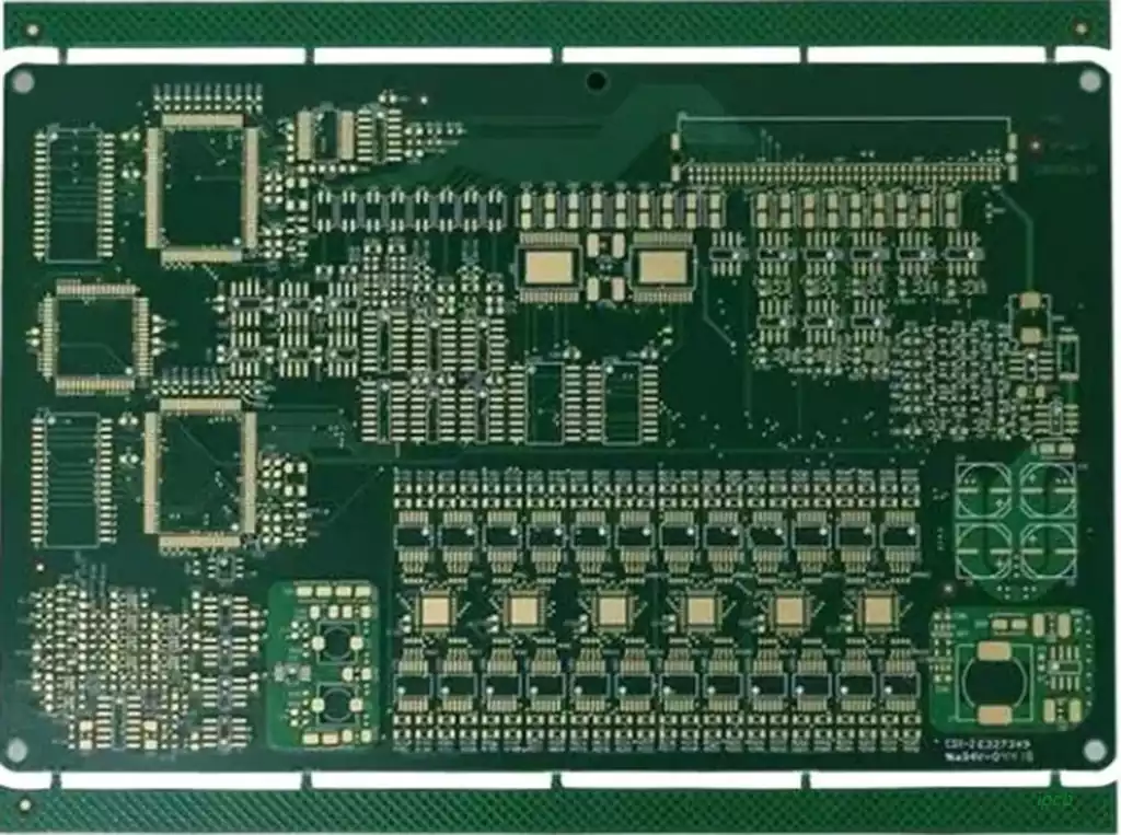
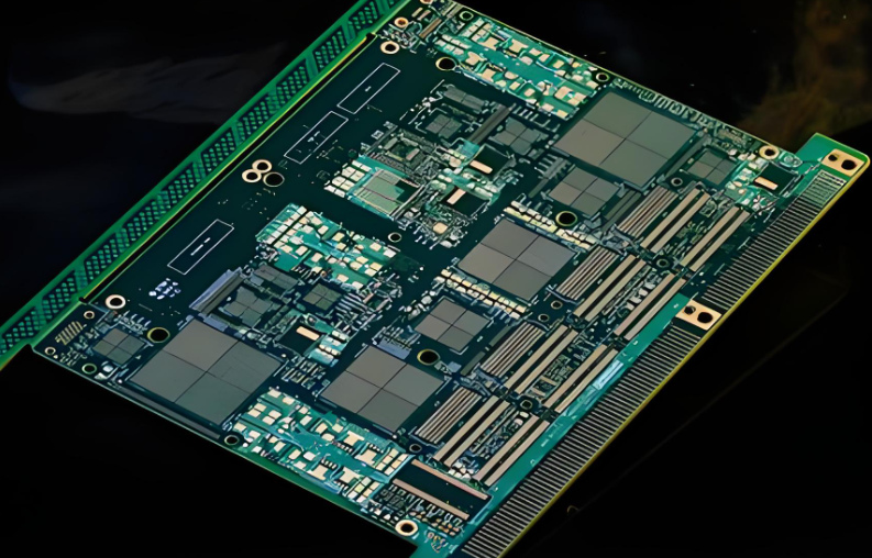
Parasitic inductance is an inductance that is not intended to be introduced by the design,but occurs naturally as an additive effect on certain objects.In short, it is always present wherever a wire is located,but its magnitude varies depending on the characteristics of the wire.For example,straight wires usually produce less parasitic inductance than coiled wires.In the case of power supply system PCB wiring,for example,each wire carries a certain amount of inductance.In practice,it is often necessary to minimise this inductance in critical current circuits,as it can cause induced voltages when the current changes,which can damage components.
Advantages:
Energy Storage: In some applications,a parasitic inductor can be used as a small energy storage device.For example,in high frequency circuits,it can temporarily store energy, which in turn weakens current fluctuations on the power line.
Filtering: Parasitic inductors can be combined with capacitive devices to build a simple LC filter that helps to suppress noise signals or interference in a specific frequency range.
Disadvantages:
High Frequency Signal Interference: During the transmission of high frequency signals, parasitic inductors can create induced impedance, which in turn can cause signal attenuation or distortion. For high-speed digital circuits, this can lead to signal integrity problems, such as signal timing disturbances or the generation of BERs.
Power supply fluctuations: In a power distribution network, parasitic inductors and parasitic capacitors form a resonant circuit, which can cause power supply voltage fluctuations and noise, posing a threat to circuit stability.
Impaired performance of switching power supplies: In the design of switching power supplies, it can lead to increased energy loss during the switching process, as well as electromagnetic interference (EMI), which not only reduces the efficiency of the power supply, but also increases the complexity of the design.
Parasitic inductance of vias is a key factor in the PCB design process that cannot be ignored. When the current flows through the vias on the PCB, due to the geometry and distribution of the vias themselves, a corresponding parasitic inductance will be generated. This may have a certain impact on the overall performance of the circuit, so in the design, it must be accurately calculated and thorough consideration.
There are various ways to calculate the parasitic inductance of an aperture, and one of the most widely used is to use the inductance formula to estimate it. For cylindrical vias, there is a specific formula to calculate:
The formula is: [L = \frac{{\mu \cdot N^2 \cdot A}}{l}]
Where:
(L) represents the parasitic inductance in Henrys (H).
(\mu) is the magnetic permeability, which is usually taken as (4\pi \times 10^{-7}) Henries per metre for air, or according to the magnetic permeability of the particular medium.
(N) is the number of turns of the perforation.
(A) is the effective cross-sectional area of the perforation in square metres (m²).
(L) is the length of the perforation in metres (m).
Calculation steps
Determine the geometrical parameters: first define the key parameters such as the diameter and length of the aperture.
Calculate the cross-sectional area: for a cylindrical perforation, the cross-sectional area is equal to the area of a circle, i.e. (A = \pi \cdot r^2), where (r) is the radius of the perforation.
Determine the number of turns: the number of turns depends on the wiring layout around the aperture and the interlayer connections.
Select the permeability: The calculation is based on the actual permeability of the material where the via is located.
Calculate by substituting into the formula: Substitute the above parameters into the formula to get the value.
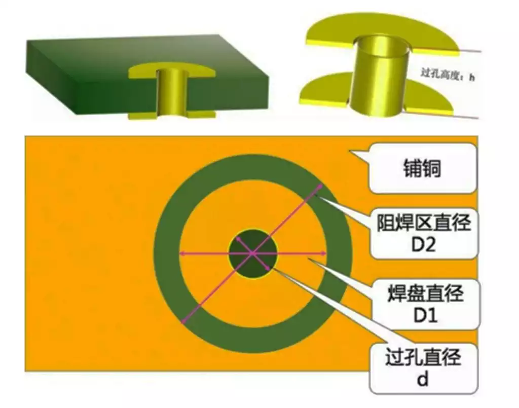
When performing the calculation, the following points should be taken into consideration:
Geometry: The geometry of the via has a direct influence on the parasitic inductance calculation, cylindrical shape is a common shape.
Material Characteristics: The permeability of different materials varies and should be calculated accurately based on the actual permeability of the material.
Number of turns and length: The number of turns and length of the perforation are important factors affecting and need to be measured accurately.
Influence factors: Parasitic inductance limits the bandwidth and speed of signal transmission, so special attention should be paid to it in the design of high-frequency circuits.
In order to reduce the impact of parasitic inductance of vias, the following strategies can be adopted in PCB design:
Reasonable layout: Avoid too dense vias and reduce the interaction between them.
Shorten the length: Try to reduce the length of the vias, thus reducing the value.
Increase the diameter: Reduce the parasitic inductance by increasing the diameter of the vias to improve the signal transmission performance.
In PCB design, the parasitic inductance of vias is a factor that needs to be carefully considered. Through reasonable calculations and design strategies, its negative impact can be effectively reduced to ensure the stability and performance of the circuit.
