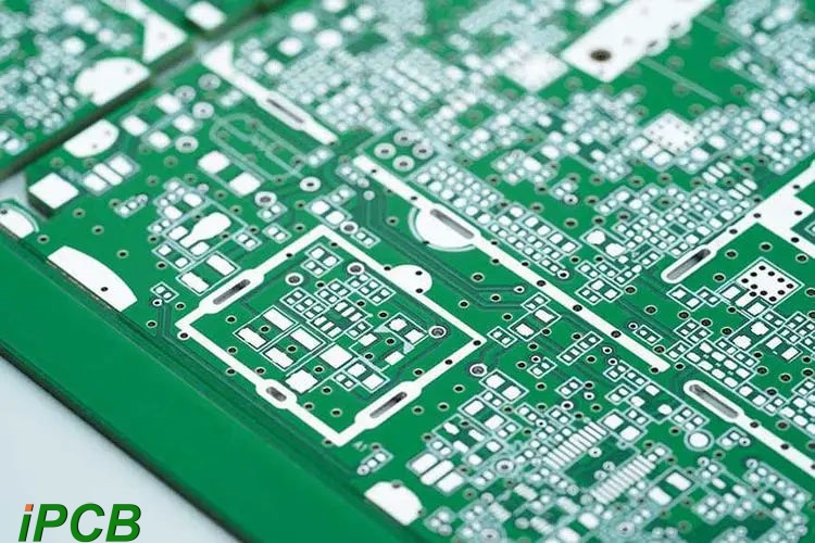
In the field of modern electronic manufacturing, with the widespread application of high-density, multi-layer PCBs, solder plugging technology has become one of the important processes to improve the performance and reliability of circuit boards.
This technology has attracted much attention because it can effectively avoid potential problems in the manufacturing and use of circuit boards. This article will explore the definition, process flow, application scenarios and future development trends of solder plugging.
Definition and function of solder plugging
Solder plugging (Solder Mask Over Bare Copper, SMOBC) is a process of sealing vias by filling solder during the manufacturing process of printed circuit boards (PCBs). This technology is mainly used to avoid problems such as solder leakage, contamination or unstable electrical performance during PCB manufacturing or use.
The main functions of solder plugging include:
Prevent solder leakage: During the soldering process, solder may leak from the via, and solder plugging can effectively seal the via to prevent solder leakage.
Improve electrical performance: Solder filling can reduce the resistance in the via, thereby improving the stability of signal transmission.
Improve mechanical strength: By filling with solder, the structural strength of the PCB is enhanced, especially in application scenarios with high mechanical stress.
Protect internal structure: Solder plugging can prevent moisture and impurities from penetrating into the PCB through the vias, thereby improving the long-term reliability of the circuit board.
Process flow of solder plugging
The implementation of solder plugging requires multiple complex and precise process steps, and the main process includes the following parts:
Design stage
When designing a PCB, engineers need to clearly identify which vias need to be solder plugged, and mark the specific location and size requirements in the design file. This step is the basis for ensuring process accuracy.
Surface treatment
Before solder filling, the PCB surface needs to be pre-treated, including cleaning, deoxidation, and chemical plating. These steps can ensure good adhesion between the solder and the hole wall.
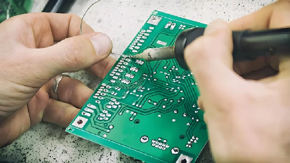
Solder filling
Solder filling is the core step of the entire process. The molten solder is injected into the pre-treated vias through special equipment. This process requires controlling the temperature, pressure and filling amount of the solder to avoid too much or too little affecting the final effect.
Surface finishing
After solder filling, the excess solder on the PCB surface needs to be removed to ensure the flatness and functional integrity of the circuit board. This step is usually completed by mechanical or chemical methods.
Quality inspection
After solder plugging is completed, the processed vias need to be inspected by optical inspection, X-ray scanning or other testing methods to ensure that the filling effect meets the design standards.
Typical application scenarios of solder plugging
With the increasing trend of miniaturization and high performance of electronic products, the application field of solder plugging technology is becoming more and more extensive. The following are several typical application scenarios:
High-speed signal transmission circuit
In high-frequency circuits, signal integrity is one of the key factors. Solder plugging technology can significantly improve the transmission quality of high-speed signals by reducing via resistance and stray inductance.
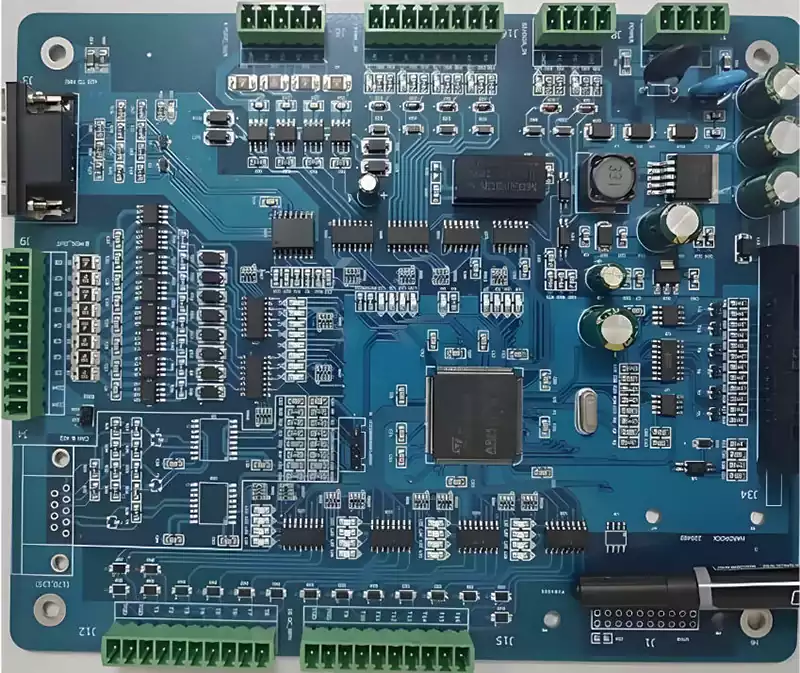
Double-sided and multi-layer PCBs
Due to their complex internal structures, double-sided and multi-layer PCBs are easily affected by solder leakage. Solder plugging can effectively block vias and avoid interference with circuit functions caused by solder penetration during welding.
Automotive electronics and industrial control
In the field of automotive electronics and industrial control, PCBs need to work in extreme environments such as high temperature, high humidity and mechanical vibration. Solder plugging technology can enhance the mechanical strength and environmental adaptability of PCBs, and is the key to improving product reliability.
Medical equipment
Medical equipment has extremely high requirements for the stability and precision of electronic components. Solder plugging can reduce internal contamination of circuit boards and improve the long-term stability and safety of equipment.
Technical challenges and solutions for solder plugging
Although the advantages of solder plugging technology are significant, there are still certain technical challenges in practical applications:
Uneven solder filling
During the filling process, equipment or material problems may cause uneven distribution of solder, affecting the filling effect. Solutions include optimizing filling equipment, improving process parameters and selecting high-quality solder materials.
Cracking caused by thermal expansion
The difference in thermal expansion coefficients between solder and PCB materials may cause cracking of the hole wall. This problem can be solved by optimizing the solder composition and controlling the process temperature.
Compatibility of high-density circuit boards
In high-density circuit boards, the via size is small, and the process difficulty of solder plugging increases. The use of micro-machining technology and advanced filling equipment can effectively solve this challenge.
Key points for quality control of solder plug holes
In the manufacturing process of solder plug holes, ensuring product quality is a key goal. The following are some core points of quality control:
Process monitoring: Real-time monitoring of temperature, pressure and filling speed during solder filling to ensure that process parameters remain within the optimal range.
Detection methods: Use technical means such as X-ray, ultrasonic detection or three-dimensional optical detection to ensure uniform solder filling without bubbles or voids.
Material selection: Select high-purity solder and high-quality substrate materials to improve the reliability and durability of the process.
Standardized process: Establish unified production standards and operating specifications to reduce the impact of human errors on product quality.
Environmental protection requirements and solutions for solder plug holes
With the increasingly stringent environmental regulations, the solder plug hole process needs to take into account environmental protection needs in material and process design.
Application of lead-free solder: Traditional solder contains lead, which has potential hazards to the environment and human health. The promotion and application of lead-free solder is an inevitable trend in the industry.
Resource utilization optimization: By optimizing the amount of solder used and reducing material waste, we can improve resource utilization efficiency and reduce production costs.
Waste treatment: Establish a complete waste recycling and treatment system to avoid environmental pollution caused by hazardous waste generated during the production process.
Technical details of solder plugging
Process control of filling solder
In the process of solder plugging, the uniformity and stability of the filling solder are the core elements. This not only affects the physical filling effect of the via, but also affects the subsequent electrical performance. In order to achieve high-quality filling, the following technical details need special attention:
Solder temperature control
Solder needs to remain molten within a suitable temperature range to ensure filling fluidity. Too high a temperature may cause solder oxidation, while too low a temperature will affect its fluidity and filling effect. Therefore, precision temperature control equipment is usually used to monitor and adjust the filling process in real time.
Via design optimization
The diameter and depth of the via directly affect the difficulty of solder filling. In the design stage, the ratio of the hole diameter to the board thickness should be considered to avoid the problem of shallow filling or solder overflow. At the same time, the roughness of the hole wall surface will also affect the adhesion of the solder. The adhesion effect can be improved through proper chemical plating treatment.
Negative pressure assisted filling
In order to ensure that the solder can fully penetrate into the via, advanced solder plugging equipment usually adopts negative pressure assisted filling technology. This method helps the solder flow into the hole faster and more evenly by applying negative pressure on the other side of the via, reducing the generation of voids.
Solder quality inspection standards
High-quality solder plugging must pass strict quality inspections. The following are commonly used inspection methods:
Microscope inspection: used to observe the uniformity and surface finish of solder filling.
X-ray inspection: non-destructive inspection of the filling state inside the via to ensure that there are no bubbles or unfilled areas.
Electrical performance test: verify whether the conductivity of the via meets the design requirements, and the impact of the filling process on the overall circuit performance.
Future development trend of solder plugging
Intelligent manufacturing and automated control
With the promotion of Industry 4.0, the solder plugging process is gradually moving towards intelligence and automation. For example, by introducing machine vision technology and AI algorithms, real-time monitoring and defect identification can be achieved, thereby significantly improving production efficiency and product qualification rate. In addition, the application of automated robot systems will further reduce the uncertainty in manual operations and reduce human errors.
Exploration of the application of new materials
Traditional solder materials are mainly tin-lead alloys, but with the continuous strengthening of environmental protection regulations, lead-free solder has gradually become the mainstream. In the future, solder materials with the following characteristics will receive more attention:
High conductivity
New alloy materials can provide better conductivity while ensuring environmental protection to meet the needs of high-speed signal transmission.
Low melting point characteristics
Developing low melting point solder materials can reduce thermal damage to the circuit board substrate during welding and improve process compatibility.
Environmentally friendly materials
Such as nanomaterials and bio-based solder materials can find a balance between performance and sustainable development.
Cross-process integration technology
Solder plugging technology may be combined with other PCB manufacturing processes in the future to form a more efficient integrated solution. For example:
Integration of laser drilling and solder plugging: Solder filling is performed directly after drilling, saving process time and improving accuracy.
Linking the electroplating process with the plugging process: After solder filling, the inner wall of the via is electroplated to enhance the conductivity and mechanical strength of the via.
Expansion of application fields
With the continuous development of the electronics industry, the application scope of solder plugging technology will be further broadened. For example:
5G communication equipment
High-speed signal transmission places higher demands on circuit boards, and solder plugging technology will play a key role in this field.
New energy vehicles
In the battery management system of new energy vehicles, PCBs need to withstand high temperatures and strong currents, and solder plugging technology can provide a more reliable solution.
Smart home devices
With the popularization of smart homes, miniaturized and highly reliable PCBs have become mainstream, and solder plugging technology will help the rapid development of this field
Summary
As an important process in the field of electronic manufacturing, solder plugging technology has played an indispensable role in improving PCB quality and reliability with its excellent performance and wide range of application scenarios.
With the continuous innovation of technology and the continuous growth of industry demand, the future development of solder plugging technology is full of infinite possibilities. In actual applications, through scientific process design and advanced equipment support, enterprises can give full play to the technical advantages of solder plugging and provide solid guarantees for the manufacture of high-quality electronic products.