Ate in pcba testing means testing the electrical conductivity and input-output values of the PCBA circuit board with mounted electronic components. In the design of the PCB circuit board, there are numerical relationships such as voltage and current between different test points. It is necessary to use professional testing equipment or manually operate a multimeter to test the test points to verify whether the actual PCBA board meets the design requirements. PCBA testing is a key step to ensure the quality of production delivery. FCT test fixtures are made according to the test points, programs, and test steps designed by the customer, and then the PCBA board is placed on the FCT test stand to complete the test.
PCBA test principle
The test points on the PCBA board are connected through the FCT test stand to form a complete path, connect the computer and the burner, and upload the MCU program. The MCU program will capture the user’s input action (such as pressing the switch for 3 seconds), and control the on and off of the adjacent circuit through calculation (such as LED flashing) or drive the motor to rotate. By observing the voltage and current values between the test points on the FCT test stand, and verifying whether these input and output actions are consistent with the design, the test of the entire PCBA board is completed.
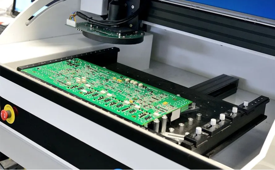
PCBA test stand
Testing must be performed on large quantities of PCBA boards, and corresponding test stands (Fixtures) are generally issued to assist in efficient completion. The principle of the test stand is to connect the test pins with the test points of the PCB board. When powered on, key data such as voltage and current in the circuit are obtained and displayed on the display screen of the test stand to achieve the purpose of rapid detection. When customers design PCB boards, engineers will consider their test plans, reserve PCB test points, and issue professional test documents or test plans to manufacturers.
Our company can make PCBA test stands by itself (equipped with engraving machines and test stand assembly engineers).
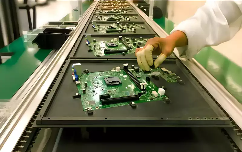
Printed circuit board assembly, also known as “PCBA”, involves a series of processing steps to install or place electronic components on printed circuit boards. PCBA first prints solder paste onto the circuit board with a template, and then places components of different types, functions and sizes on the pre-printed solder paste. The next step is to reflow the circuit board with components to fully cure the solder paste and achieve reliable connections. The assembled circuit board is then inspected using an automatically operated high-speed machine and a visual system.
The assembly process of PCBA does not end after optical inspection. A PCB may look good but be electrically defective. This is where PCBA testing comes in handy. PCBA testing is the electrical testing of assembled boards to screen for manufacturing defects, material defects, or board design issues.
Types of PCBA testing
- In-circuit testing (ICT)
The first type of PCB assembly testing most commonly used for high-volume PCBA production is in-circuit testing (ICT). In-circuit testing is a bed-of-nails type PCB assembly test that tests PCB contact points simultaneously with a custom fixture. For in-circuit board assembly testing, both diagnostic and test times are relatively fast. The disadvantage of ICT is that it is less flexible because it can only cater to a single type of PCB and is expensive because of its complex software program and expensive tools. In-circuit testers can be used independently or integrated with functional test systems for more efficient fault coverage and throughput. - Flying probe testing
A more flexible type of testing is called flying probe testing which uses probes that can move or fly to test PCBs. It can test fine-pitch devices but is relatively slower than ICT, making it more suitable for prototyping and small-scale production. It has a short development time and can be easily modified based on changes in the PCB layout, while ICT requires expensive tester modifications. - Functional Testing
The third type of circuit card assembly testing is called functional testing. This method of board assembly testing takes longer because all functions of the board need to be tested to ensure that the board works as required by introducing stimuli and measuring the board’s response. Functional board assembly testing is also very expensive to design and develop.
However, please note that it is impossible to have 100% test coverage of all components due to important factors such as stray impedance, cost, and processing time. To increase confidence in test coverage, PCBA companies sometimes implement ICT and functional testing at the same time.
4.ate in pcba testing
Other processes and offline controls in the assembly process, such as stencil printing inspection, automated optical inspection (AOI), and X-ray inspection, must also be implemented to further strengthen the quality of the PCB. Each inspection process is described in detail below:
- Stencil Printing Inspection (SPI)
After the solder paste is printed on the PCB with a stencil, the position, volume, and shape of the solder paste are checked with a stencil printing inspection machine. The solder paste volume is measured relative to the aperture volume. The solder paste alignment is also checked during this inspection process and is usually measured in width and length. - Automated Optical Inspection (AOI)
Automated Optical Inspection (AOI) is a fast inspection technology that can check for missing components, misalignment, tombstones, and other visual defects that ruin the image of the PCB. Using the vision system software, a camera scans and hovers over the board using a predefined program. The captured image is compared to a reference image to identify visual faults on the PCB. Some visual parameters such as resolution, brightness, and lighting need to be controlled to balance accuracy and speed of inspection. - X-ray Inspection
Since AOI is limited to the camera’s line of sight, another inspection method is needed to “see through” the printed circuit board. X-ray inspection is an inspection process that detects problems with components and PCB interfaces. Solder quality is best inspected using X-ray inspection because it scans the solder material. Shorts caused by solder bridging and bridges are easily visible in X-ray images. X-ray technology uses the different absorption capabilities of materials to produce unique images and patterns for voids/air gaps and components. - Reliability Testing
Reliability testing is also performed, such as environmental and physical testing, which simulates the long-term application of the printed circuit board. Example Circuit Card Assembly Reliability Testing includes vibration, flexure, aging, and thermal cycling. The ability of the board to withstand stress at a specified temperature, duration, and stress level determines the reliability performance of the board. Output responses such as delamination, test readings, and warpage measurements are some of the important items that need to be monitored during these reliability tests.
Advantages of Involving PCBA Testing
- Economic Benefits
Circuit board assembly testing can detect manufacturing defects before the parts leave the assembly floor, which can bring financial rewards. If the PCBA is tested, the faulty parts will no longer be sent to the end user, thus avoiding the loss of revenue caused by customer returns, tedious analysis, and worst, accidents of unsafe parts. Although the cost of test development, hardware, software, and tester maintenance is high, circuit board assembly testing is beneficial in ensuring that only boards that meet specifications are sent to customers. - Quality Control
Quality control is essential at every stage of PCBA. Manufacturing errors caused by reflow, component placement, and stencil printing will be detected during testing. 100% circuit card assembly testing after assembly will also be able to determine if there are any loopholes in previous controls. In this way, the assembly process can be further improved to reduce test rejections. - Early Feedback System
Another major advantage of circuit board assembly testing is that it can detect problems immediately after the assembly process. Without testing, defects may be discovered later in the electronic assembly process, which may make it more difficult to analyze the problem. The cost impact of late detection is also greater because more units are produced without correcting the process immediately. Early detection will provide the printed circuit board assembly with enough time to correct the problem and control the affected products. - Customer Satisfaction
Customers expect to receive high-quality PCBs when they are shipped. Zero field failures and zero customer complaints are major quality key performance indicators (KPIs) that can only be achieved by implementing rigorous post-assembly screening. Circuit card assembly testing can effectively eliminate scrap that does not meet the electrical and functional requirements of the circuit board. If zero complaints are met, the supplier rating will be higher, creating opportunities for more orders and new product introductions.
PCBA test types are divided into the following categories:
- ICT (In-Circuit Test) test: It mainly detects the voltage/current data of the test point after the PCB circuit board is powered on, and does not involve the test of function buttons or input and output.
- FCT (Functional Test) test: It is necessary to first burn the written single-chip microcomputer (MCU) program into the program IC through a burner (such as ST-Link, JTAG) to implement the corresponding functional test. For example, after pressing a key, the LED light turns on; pressing two keys at the same time restores the factory settings, etc. Of course, whether all functional tests can be carried out must be based on the premise that the PCB is soldered OK and the circuit is conductive, otherwise it cannot be achieved.
- Burn In Test test: For the PCBA board that has been burned and passed the FCT, long-term and periodic simulation of user input and output is performed to detect its durability and welding reliability. In special cases, the PCBA board needs to be exposed to a specific temperature and humidity environment.
As the density of printed circuit boards becomes higher and higher and the size becomes smaller and smaller, the difficulty of testing is also increasing. Due to the narrow path and very limited space, the efficiency of accessing test points is getting lower and lower. These challenges can be mitigated through careful design, testing and prototyping. ate in pcba testing is an essential and important link in the entire PCBA manufacturing supply chain. Quality is controlled from the final data results. In standardized design and manufacturing management, PCBA testing must be considered and implemented.
