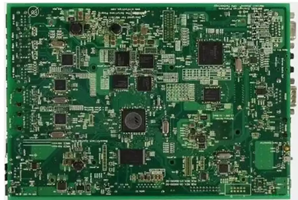
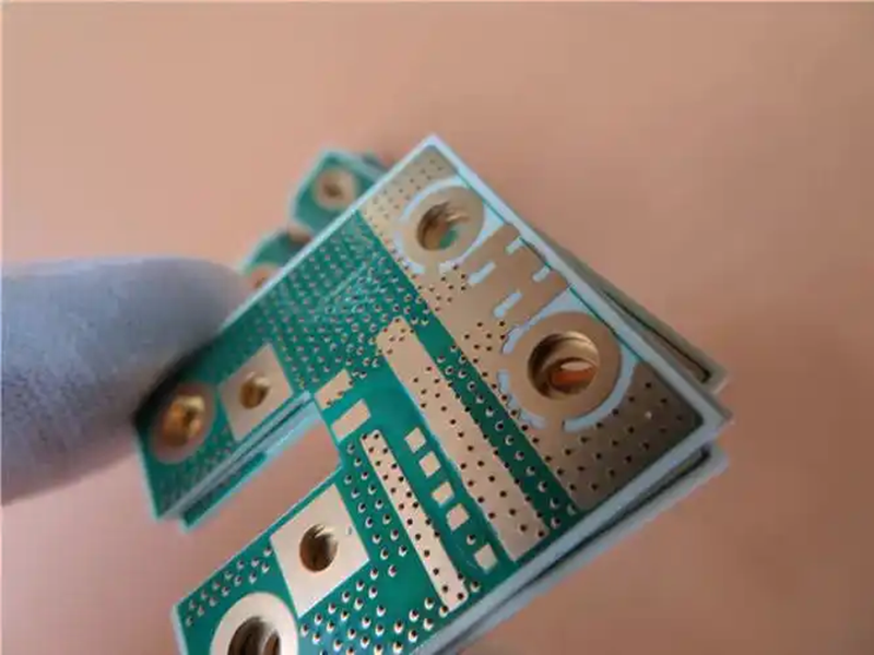
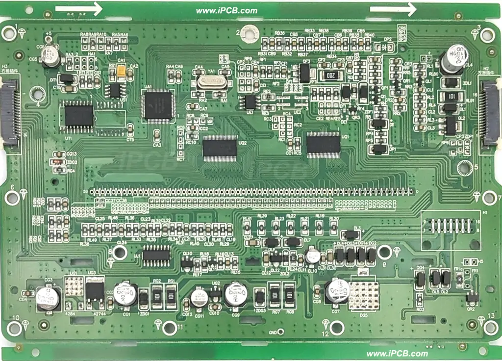
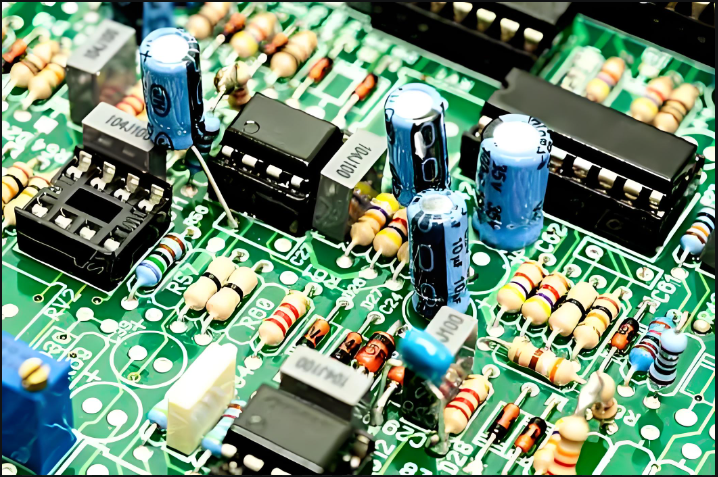
PCBA chip processing is one of the core links in the manufacturing process of electronic products, which includes a number of stages from circuit design to product moulding. Each stage needs to be carefully prepared to ensure that the production process is carried out smoothly, as well as the quality and reliability of the final product.
PCBA Processing Preparation: Design and Material Procurement
Production BOM
BOM, i.e. Bill of Materials, lists in detail all the materials required for manufacturing a complete product,covering comprehensive information such as material number, model specification,package form, bit number identification and required quantity,etc.The BOM list is an important standard document on which the SMT placement factory bases its material preparation and inspection process.
PCB source file
PCB source documents for determining the layout of components and direction is extremely critical, it can be said that the lack of these documents, the subsequent processing steps will not be able to talk about, therefore, customers must provide accurate PCB source documents. Usually, these documents should contain: component location coordinates, bit number illustration and component polarity of the clear instructions. If the original files are not available, then at least the coordinate data and bit numbering of the PCB must be provided.
Gerber File
The Gerber file plays a vital role in the SMT placement process, as it contains key data such as pads, soldermasks and silkscreen layers on the PCB. This information is essential to the stencil and placement process. It is important to note that the Gerber file is a collated piece of data, not a single board, and is used to accurately set the position, size and orientation of the stencil apertures to meet the solder paste printing requirements of the subsequent SMT placement process.
Coordinate File / Bitmap
Coordinate files are used to indicate the location information of each component on the PCB, which is often exported as a text file or Excel table format. These files are measured in millimetres and must contain the coordinates of the origin of the PCB to ensure accurate component location. Bit numbering diagrams help to visualise component polarity, and the bit numbering diagrams provided require the immediate part to be clearly labelled for accurate identification.
Sample Image
The sample image is the reference material to verify the conformity of the finished SMT chip processing product with the design. Comparison of the sample image with the actual product can identify any inconsistencies between the two.
Test Requirements
For those components that must be subjected to mandatory testing, once the test product is involved, the customer must be equipped with the appropriate test software, test procedures and test fixtures to facilitate the testing of PCBA products. If there are specific quality requirements,material selection or process standards, such as soldering quality, assembly accuracy, reliability indicators, etc.,these details also need to be submitted to the SMT placement factory before production. In addition, the SMT placement process may also require other auxiliary documents,such as layout diagrams,test operation guidelines, etc. These documents will be provided according to the actual needs to ensure that the SMT placement process is smooth and unimpeded.
SMT placement process: realising efficient automated production
According to the SMT production planning, prepare all the necessary materials, including PCB boards, component materials and stencils,and strictly ensure that the quality and quantity of these materials are up to standard. Subsequently, it enters the key link in the PCBA manufacturing process – SMT placement processing. At this stage, high-precision placement machines accurately attach small components such as chips,resistors,capacitors, etc.to the surface of the PCB. This highly automated production method greatly improves production efficiency, while significantly enhancing product quality and ensuring component accuracy and reliability.
Wave and hot-air oven soldering: guaranteeing the quality of the solder joints
Wave and hot-air oven soldering is one of the key aspects of PCBA processing and is used for soldering large components and plug-in components. In wave soldering, the PCB is washed through a wave of liquid solder to achieve soldering. Hot air oven soldering, on the other hand, achieves soldering by melting the solder through a stream of high-temperature air. Both processes guarantee the quality and stability of the solder joints.
Manual soldering and testing: ensuring quality and reliability
Even in automated production, the soldering of certain special components requires manual work.The manual soldering session usually includes steps such as adjusting the soldering parameters and checking the quality of the solder joints to ensure the quality of each solder joint. Afterwards, the PCBA boards will undergo rigorous testing, including appearance inspection, function testing, etc., to ensure the quality and reliability of the product.
Post-assembly and packaging: presenting perfect electronic products
Finally, the PCBA board will undergo post-assembly, including mounting the shell, connecting cables, installing accessories, etc. After assembly, the product will be finely packed to protect the product from damage during transport and use. Good packaging not only improves the appearance of the product texture, but also provides a better user experience.
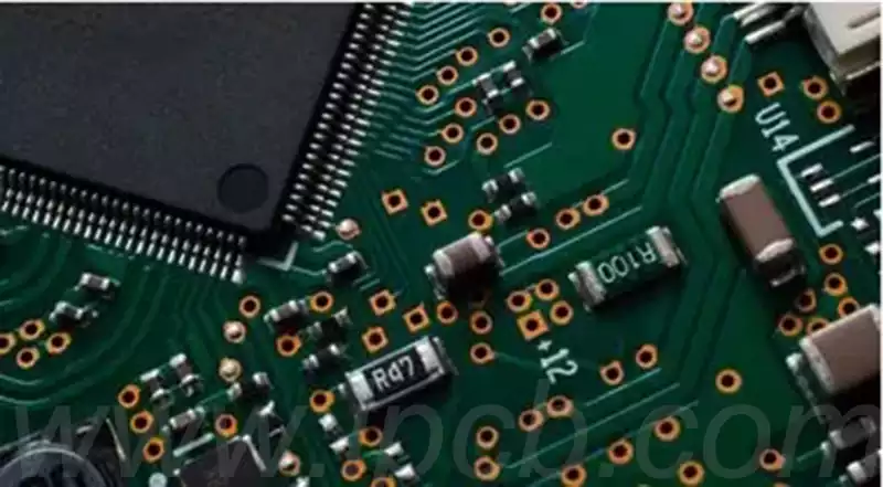
Precautions in the process of PCBA processing and production
1.Design stage
In the PCBA processing and manufacturing process, the design phase plays a pivotal role. The core task of the design stage covers the layout planning of the PCB board, the selection and layout of components, the path planning and connection means and other aspects. In the design phase, the following points need special attention:
(1) Component selection: the correct selection of components is to ensure the quality of the circuit board is a key link. In the selection process, careful consideration should be given to the brand, model, package form and various parameters of the components, as a basis to ensure the quality and stability of the components.
(2) PCB circuit board design: the design of PCB circuit boards, need to comprehensively consider the size of the component specifications, layout arrangements, line paths and connection methods and other elements. The design process should follow the principle of scientific layout, effectively avoiding mutual interference between components, thereby ensuring the stability and reliability of the circuit board.
(3) anti-static measures: in the design and manufacturing process of PCB circuit boards, must attach great importance to static electricity protection. The actual operation, should be equipped with anti-static gloves, electrostatic mats and other protective equipment to eliminate electrostatic interference, to avoid damage to components.
2.In the PCBA processing and production of manufacturing links:
(1) PCB circuit board production:The production of PCB circuit boards, need to ensure that the board surface with a high degree of smoothness and flatness, in order to prevent unevenness due to the board surface and trigger the problem of component welding is not secure.
(2) Component assembly:The assembly of components should be precise and accurate to ensure that their position and attitude are in accordance with the design requirements, to avoid damage to the circuit board or its functional failure due to positional deviation or attitude errors.
(3) Soldering process:When performing soldering operations, the temperature and time should be strictly controlled to prevent damage to the components due to high soldering temperature or long duration.
(4) Quality inspection:In the PCBA processing and production process, quality inspection is an indispensable part, covering the welding quality of components, line connection status and other aspects. Inspection, with the help of professional testing instruments and equipment,in order to protect the quality and reliability of the product.
3.In the encapsulation stage of PCBA processing and production:
(1) Selection of encapsulation materials:The selection of encapsulation materials should be based on the performance specifications of the product and the actual use of the environment, such as the consideration of its high temperature resistance, thermal shock and dust and other characteristics.
(2) Temperature control and duration management during encapsulation:In the encapsulation process, the temperature and time parameters must be strictly monitored to prevent degradation of the encapsulation material or decline in the overall product performance due to excessively high temperatures or long durations.
(3) Encapsulation of the airtightness guarantee:Encapsulation of the airtightness of the maintenance of product stability and reliability is critical, so in the encapsulation process, we must ensure that the required airtightness standards.
4.In the test phase of the PCBA processing and production process:
(1) Selection of test instruments and equipment:Appropriate test instruments and equipment should be selected based on the performance characteristics and specifications of the product to ensure the accuracy and reliability of the test results.
(2) Configuration of test parameters:The setting of test parameters should closely match the performance requirements and specifications of the product to ensure the accuracy and reliability of the test results.
(3) Evaluation and recording of test results:The evaluation and recording of test results must strictly follow the product testing guidelines to ensure the accuracy and reliability of the test results.
