Hybrid Bonding is an advanced IC packaging technology used to achieve high-density, high-performance interconnections between different chips. The key feature of this technology is to replace the traditional bump or solder ball (bump) interconnections with direct copper-to-copper connections, which enables ultra-fine pitch stacking and packaging in a very small space for the purpose of three-dimensional integration.
In the hybrid bonding process, metal layers (usually copper) of two or more chips are precisely aligned and pressed directly together to form a direct electrical contact. In order to ensure a good connection, special treatments are required on the surface of the chips, such as the deposition of a layer of dielectric material (e.g., Si02 or SICN) with a homogeneous eye pattern, on which copper pads and chattering holes (TSVs) are prepared at micron to nanometre scales. These pads and vias connect the circuitry inside the chip to the outside, enabling faster data transfer, lower power consumption, and greatly enhancing the integration of the chip.
Prior to the advent of hybrid Bonding, 2D, 2.5D and 3D packages relied on solder bumps or micro bumps to make the electrical connections between the chip and the substrate, the chip and the interposer, and the chip. These solder balls are implanted on copper bumps to complete the electrical connections. As the copper post pitch shrinks to less than 10~20 microns, the difficulty of the solder ball preparation process increases dramatically, and the defect rate also rises, becoming a bottleneck that restricts high-density packaging.
In order to solve the chip bonding problem of less than 10 micron pitch, Hybrid Bonding came into being. This technology not only achieves direct bonding of copper bumps at room temperature, but also tightly fits the non-conductive areas of the chip face-to-face, eliminating the gaps in the traditional solder ball connection and avoiding the need for epoxy filling.Hybrid Bonding is highly regarded and widely demanded by the industry because of its excellent electrical performance and low signal loss, which makes it particularly suitable for the field of high-throughput and high-performance computing. Hybrid Bonding
Originally known as DBI (Direct Bond Interconnect), Hybrid Bonding was proposed in the mid-1980s at the Research Triangle Institute (RTI) laboratories by Paul Enquist, Q.Y. Tong, and Gill Fountain, who founded Ziptronix, Inc. in 2000, and in 2005 founded the company Ziptronix. Ziptronix, which achieved 10 µm pitch DBI bonding of aluminium wiring layers in 2005, followed by 2 µm pitch wafer-to-wafer bonding in 2011.In 2015, Ziptronix was acquired by Xperi (formerly Tessera), and in 2019 Xperi completed a patent on its DBI/Hybrid Bonding technology layout, but the technology has not yet achieved large-scale mass production.
Principles of Hybrid Bonding
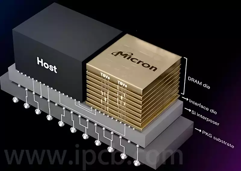
- Interchip Bonding
In the process of interchip bonding, multiple chips are connected to the package substrate using, for example, metal cables.
The connection between chips with different functions can be realised to expand system performance and functions. - Intra-chip bonding
Intra-chip bonding refers to bonding inside a single chip to realise the connection between different functional units.
It can improve the internal integration of the chip, reduce the signal transmission delay, and improve the performance. - Bonding Advantages
Hybrid bonding combines the advantages of inter-chip and intra-chip bonding to achieve efficient interconnections between chips and chips and within chips.
It meets the connection needs between different functional modules and improves integration and performance.
The hybrid bonding process, which forms the bonding interface layer, usually consists of Cu/SiO2, but it easily leads to the generation of Cu2O, which is released under the action of an electric field
and diffuses into the insulating material of SiO2, where leakage occurs. Sometimes it is necessary to coat a layer of SiCN on top of SiO2 as a barrier layer.
At present, the most suitable machine for Hybrid Bonding in the world for mass production is the Austrian company EVG, such as the GEMINI series of bonding machines. Its advantage lies in SmartView’s Face-to-Face alignment module, as well as alignment verification module.
As technology continues to advance and application needs increase, hybrid bonding technology is evolving in several directions:
Diversified bonding methods: In the future, hybrid bonding technology will further expand the types and combinations of bonding methods to meet the needs of more materials and processes.
Refined bonding process: with the continuous development of microelectronics manufacturing technology, hybrid bonding process will achieve higher precision and smaller size to adapt to the miniaturisation and high performance packaging needs.
Intelligent bonding equipment: Intelligent bonding equipment will achieve automation and intelligent production, improve production efficiency and product quality, and reduce production costs.
Green: hybrid bonding technology will pay more attention to environmental protection and sustainable development, using low energy consumption, low pollution, recyclable processes and materials, to contribute to green manufacturing.
Hybrid bonding achieves high-density interconnections without gaps between chips through precision alignment and direct pressing of copper and dielectric layers. In the future, with the continuous optimisation of the process and the intelligent development of equipment, hybrid bonding will play a role in a wider range of applications. Its process details and material selection will also be more diverse to meet different chip design and system requirements.