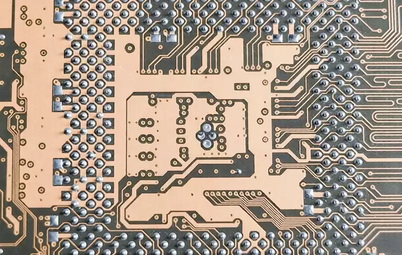
PCB test points may look like just some pads or exposed copper skins, but their role in the entire production, debugging, testing and repair process is very critical. If the test points are not reasonably arranged, it will lead to difficult to test the circuit board, debugging time becomes longer, the difficulty of rework increases, and even cause a reduction in the yield rate, affecting the delivery cycle of the product.
Most electronic products are subjected to functional, electrical performance and automation tests before they leave the factory. In order to complete these tests efficiently, engineers need to arrange suitable locations on the PCB as probe contact points. These locations are pcb test points. They can connect signal lines, power lines, ground lines, I/O pins and other key nodes, and are used to detect whether there are open circuits, short circuits, signal abnormalities and other problems.
If there is no test point, the test probe cannot reliably contact the circuit, the device cannot read the signal, and there is no way to determine whether the circuit is working properly. In this way, it can only be measured by manual means, which is not only inefficient, but also prone to errors. In small quantities or prototype development stage, manual testing can barely cope. But in mass production, the reasonableness of the test point layout is directly related to the production rhythm of the whole factory.
Common types of pcb test points:
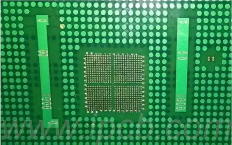
- Pads as test points
Some chips are directly exposed pins, pads, can also be used as a test point. The probe of the test equipment can directly contact these positions. This way is simple and suitable for low density boards with fewer SMD components. - Individual test pads
Design special round test pads for probe contact only. These pads do not connect to components but only to signal lines or power rails. Commonly used in automatic test fixtures. - Pin Test Holes
Design a through-hole to insert a probe for testing. This type of hole should be large enough for the test pin to be inserted, but it should not affect the circuit function. Suitable for THT boards or manual test occasions. - Edge Test Points
Place gold fingers or exposed copper surfaces on the edge of the PCB for probe clamping or contact. This method is suitable for testing of connectors and interface circuits.
Different types of pcb test points are suitable for different testing methods, according to the product to choose the appropriate programme.
The basic principles of pcb test point layout in PCB design
A reasonable test point layout not only improves the efficiency of circuit testing, but also effectively reduces the risk of debugging and production process. The following are some of the basic principles to follow when the pcb test point layout:
- Ensure the accessibility of test points
Test points should be located in easily accessible locations, avoiding being obscured by other components or alignments. Test points should try to avoid being set up in places that are difficult to reach, especially after other components have been installed, and test points should be able to be easily connected to the test equipment. - Avoid Test Points Interfering with Signal Paths
In the path of high-speed or analogue signals, avoid setting up test points in the signal path. Test points, if not properly designed, may introduce additional electromagnetic interference and cause signal distortion. Test points should be kept as far away as possible from the signal alignment to avoid introducing noise. - Reasonable setting of power supply and ground test points
Power supply and ground test points should be close to the power supply input and keep a short connection path to the power supply chip and ground plane. Avoid the power supply test point being too far away from the power supply voltage source, so as not to cause power supply voltage drop or interference. - Selection of test point spacing and size
The spacing and size of test points need to be designed according to actual needs. For smaller test equipment (e.g., pin probes), appropriate test point diameters (generally 0.8mm to 1.2mm) should be designed. The spacing between test points needs to be adjusted according to the layout of the PCB and the requirements of the test equipment. - Labeling test point functions
Each test point should be clearly labelled with its function and corresponding signal. By labelling the function name, signal name or number, etc., it helps engineers to identify and use the test points quickly. - Avoid placing test points in the soldering area
In the soldering area of the PCB, designers should try to avoid placing test points. This is because the soldering process may produce solder splatter, affecting the reliability of the test point. Test points in the soldering area should be avoided as much as possible, or use special protective measures.
PCB Test point LAYOUT Note:
- General test point size are 30-35mi, component distribution is denser, the pcb test point can be as small as 30mil.
The distance between the test point and the component PAD is at least 40mil. - The distance between the test point and the test point is at least 50-75mil, 75mil is generally used, and 50mil can be used when the density is high.
- Test points must be evenly distributed on the PCB to avoid uneven stress on the board surface during testing.
- Multi-layer boards must leave the test points on the solder side through the IA holes.
- Test points must be placed in the Bottom Layer.
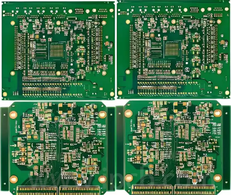
PCB test point is an indispensable element of circuit board design, its reasonable layout directly affects the test efficiency, debugging time and product quality. Fully consider the type of test points, layout principles and considerations, is to ensure high performance and high yield of electronic products is the key.