Photoresist, also known as photo-resistive material, refers to an etch-resistant thin-film material whose solubility changes upon exposure to ultraviolet light, electron beams, ion beams, X-rays, or other forms of radiation.
Photoresist comprises photosensitive resin, photoinitiators, solvents and additives: photoinitiators, also known as photopolymerisation materials (primarily including UV coatings, UV inks, UV adhesives, etc.), are materials that initiate polymerisation upon exposure to light.
Photoresist comprises photosensitive resins, photoinitiators, solvents, and additives: Photoinitiators, also termed photopolymerisation materials (primarily including UV coatings, UV inks, UV adhesives, etc.), constitute the photosensitive component within photoresist materials. They undergo photochemical reactions, absorbing specific wavelengths of energy within the ultraviolet or visible light spectrum to generate free radicals, cations, and other species, thereby initiating the polymerisation and cross-linking of monomers to form cured compounds. Photoinitiators are the pivotal component of photoresist, decisively influencing its photosensitivity and resolution.
Photosensitive resins constitute the primary component of photoresist, providing structural support. They serve to polymerise disparate materials within the photoresist matrix, conferring etch resistance and determining fundamental properties such as hardness, flexibility, and adhesion.
Resin synthesis techniques encompass radical polymerisation, anionic polymerisation, and reactive radical polymerisation. Radical polymerisation is currently the most prevalent method, whilst reactive radical polymerisation remains unindustrialised.
Solvents constitute the largest component in photoresist, serving to maintain its liquid state. The solvents themselves exert negligible influence on the photoresist’s chemical properties. Additives are typically proprietary compounds employed to modify specific chemical characteristics of the photoresist.
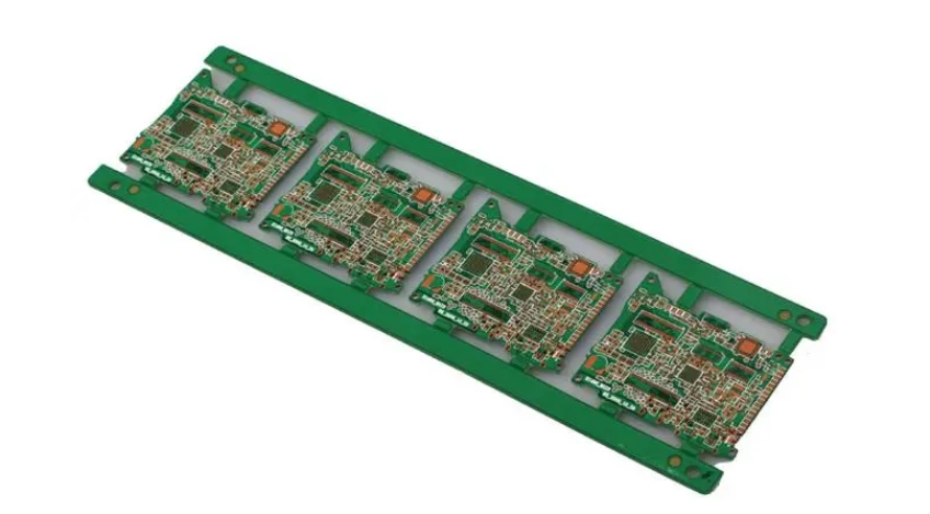
Photoresist plays a crucial role in printed circuit board manufacturing. It protects areas of the board that are not to be etched, allowing only the designated regions to reveal the required pattern. This ensures the accuracy and precision of the etching process.
Concurrently, the quality of the photoresist directly impacts both the quality of the circuit board and production efficiency. Therefore, during the manufacture and application of photoresist, strict control over process parameter adjustments and quality standards is essential.
Method for Manufacturing Photoresist PCB Boards
- Photoresist Formulation
Photoresist for printed circuit boards primarily consists of polyester or epoxy resin, with its core formulation comprising three key components. Firstly, the photosensitiser efficiently absorbs ultraviolet light to initiate photochemical reactions, thereby precisely delineating the desired circuit patterns. Secondly, sunflower oil, when combined with the photosensitiser, not only accelerates rapid curing under intense light but also significantly enhances the photoresist’s mechanical strength.
Thirdly, solvents are incorporated to regulate the photoresist’s physical properties. When mixed with diluents, solvents effectively reduce viscosity, facilitating uniform coating on circuit board surfaces and ensuring precision in subsequent processes. The synergistic interaction of these three components forms the foundation for the photoresist’s functionality.
Precise control over the proportions and properties of these constituents is crucial for the photoresist’s ultimate performance. An optimised formulation ensures the photoresist exhibits ideal reactive characteristics and physical properties under illumination, laying the groundwork for high-quality circuit board manufacturing.
- Photoresist Mixing
The photoresist preparation process involves blending photosensitiser, sunflower oil, and diluent in specific proportions. To ensure mixture homogeneity, this step requires stirring and degassing. These procedures yield a stable, uniform photoresist mixture. - Photoresist Application Methods
Applying the mixed photoresist onto the circuit board surface commonly employs methods such as coating, spraying, and spin coating. Within semiconductor manufacturing technology, spin coating is currently one of the prevalent techniques for forming photoresist layers on semiconductor wafers. During application, the wafer is positioned face-up, coated with photoresist, and then subjected to high-speed rotation to achieve uniform distribution across the wafer surface.
Spin Coating Method
Spin coating is a common and crucial technique in photoresist application, ensuring uniform layer thickness and defect-free coverage.
Specific Steps: The process involves spraying photoresist onto the silicon surface, followed by rotating the semiconductor wafer to remove excess material while evaporating solvents within the layer, thereby achieving consistent thickness.
Advantages and Challenges: This method achieves uniform photoresist films using minimal material. However, conventional spin coating often produces microscopic bubbles near wafer edges. These bubbles may cause damage during subsequent etching processes, forming pits approximately 4000 angstroms in diameter and 1000 angstroms in depth. To address this issue, methods have been proposed involving pre-treatment prior to resist coating. This includes applying organic solvents to the semiconductor wafer surface to prevent bubble formation within the resist layer.

Application details: During spin coating, the wafer rotation speed typically ranges from 0 to 500 rpm, with 200 to 500 rpm being optimal. Resist volume is determined by the required layer thickness and photolithography/etching process parameters (e.g., line width).
Alternative coating methods
Beyond spin coating, other techniques exist:
Spray Method: Spraying organic solvents involves directing the solvent onto the central or near-central region of the semiconductor wafer surface. The nozzle moves to a position above the wafer’s centre or near-centre area, dispensing the organic solvent while the wafer is stationary or rotating. This method helps reduce resistance to photoresist flow on the wafer surface during subsequent processes, thereby minimising photoresist consumption.
Immersion method: In certain photoresist stripping techniques, the array plate may be directly immersed in a photoresist stripping solution.
Coating systems: Modern photoresist coating systems enable rapid switching between different photoresists using the same nozzle. This is achieved by controlling the nozzle to clean within a cleaning cylinder before drawing up another photoresist, thereby simplifying operations and enhancing efficiency.
Photoresist serves as a critical material in microelectronics manufacturing, forming patterns on circuit boards through photochemical reactions. Comprising photosensitive resins, photoinitiators, solvents, and additives, its production demands precise formulation and uniform coating techniques. Photoresist quality directly impacts circuit board performance, rendering stringent quality control essential.