In RF circuit design, signal interference, power supply noise, and mutual interference between components often become critical factors limiting system performance. Through scientific and rational partitioning design, effectively separating circuit modules with different functions can not only significantly reduce signal interference but also greatly enhance system stability and reliability.
- Physical Zone Segmentation
① Component Layout Planning:
High-frequency component separation: Isolate high-frequency components (e.g., amplifiers, mixers) to minimize mutual electromagnetic interference.
Separate Input/Output Port Placement: Ensure RF input and output ports are spatially separated to prevent signal feedback and interference.
Filter and Antenna Layout Planning: Position filters near antennas to minimize signal loss and interference; simultaneously maintain appropriate distances between antennas and other high-frequency components.
② Shielding and Isolation Measures:
Application of Metal Shielding Cages: Enclose susceptible components like high-power amplifiers and mixers with metal shielding cages to isolate external electromagnetic interference.
Ground Plane Partitioning: On printed circuit boards, use ground planes to separate functional zones, reducing signal crosstalk.
- Electrical Zone Partitioning
① Power and Ground Management:
Independent Power Supply: Provide mutually isolated power sources for different functional modules to prevent power noise propagation between modules.
Optimal Decoupling Capacitor Placement: Position decoupling capacitors near each power pin to filter high-frequency noise and maintain power purity.
Optimized High-Current Path Design: Design wider traces for high-power components and incorporate multiple vias to ensure even current distribution and minimize voltage drop.
② Signal Path Management:
High-Frequency Trace Routing: Route high-frequency signals along the shortest path, avoiding right-angle turns to reduce transmission loss and interference.
Impedance matching: Implement impedance matching along signal transmission lines to preserve signal integrity and minimize reflections.
Filter signal path planning: Ensure the shortest possible path for signals passing through filters while maintaining effective isolation between filter inputs and outputs to prevent signal leakage and interference.
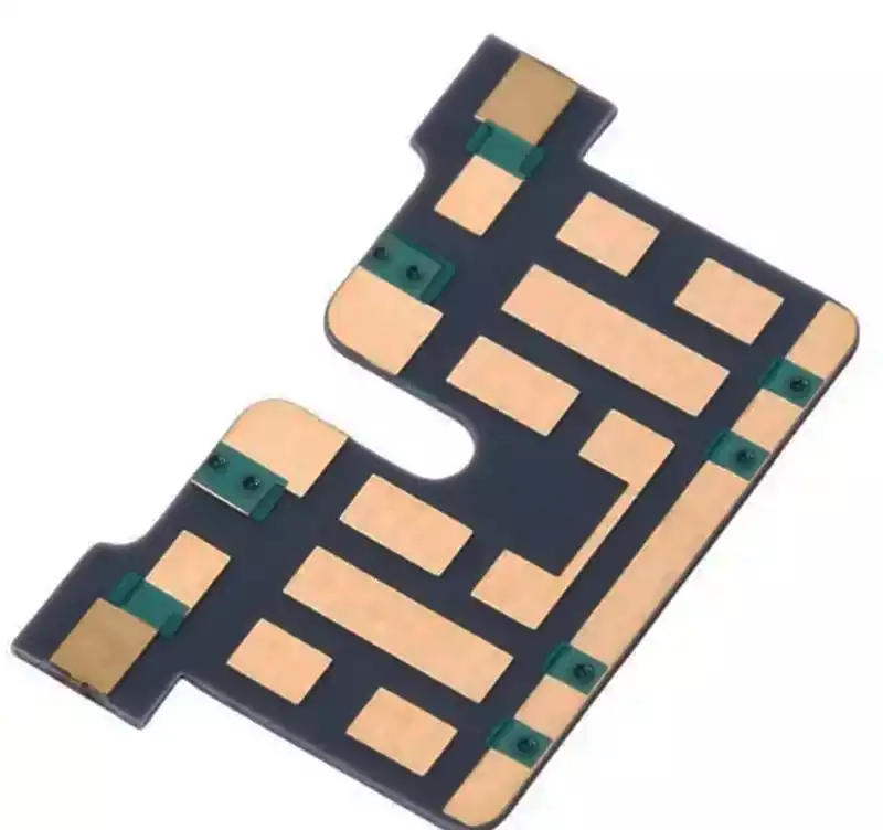
RF PCB partitioning: Separating functional circuit modules reduces signal interference and enhances system stability. Key benefits include:
Reducing Electromagnetic Interference
Physically isolating high-frequency signals (e.g., RF, high-speed differential pairs) from low-frequency signals (e.g., digital I/O, analog signals) prevents capacitive coupling or impedance mismatch interference caused by bends or parallel lines. For instance, using 135° arc transitions for high-frequency differential lines reduces reflections, while maintaining differential line length differences within 0.3mm prevents phase shifts.
Optimizing Signal Integrity
Positioning core components (e.g., MCUs, power amplifiers) at the geometric center shortens signal paths to peripheral components. For instance, a temperature sensor PCB improved measurement accuracy from ±1°C to ±0.1°C by reducing signal paths by 3cm.
Enhancing Power Stability
Employ rf circuit design with adjacent power and ground planes to achieve effective capacitive coupling, reducing power supply noise interference. For instance, high-current power lines utilize multilayer boards to minimize voltage drop, ensuring stable power delivery to high-power amplifiers.
Isolating Sensitive Components
Position low-noise amplifiers and high-power amplifiers on separate layers or zones, isolating them with metal shields to prevent electromagnetic radiation and thermal conduction interference.
The partitioned rf circuit design represents a systematic and meticulous endeavor. Through dual optimization at both physical and electrical levels, it constructs a low-interference, high-stability operating environment for RF systems. From the careful arrangement of electronic components to the ingenious application of shielding and isolation measures, from the precise management of power and ground planes to the exact control of signal paths—each step embodies the wisdom of pursuing ultimate performance.