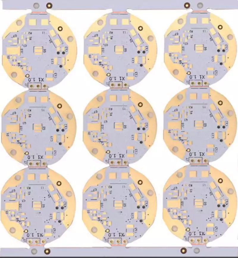
As a core material for high-reliability electronic components, the production process of multilayer aluminium substrates integrates precision machining with materials science, with each step directly impacting the product’s electrical performance and mechanical stability. From substrate surface pre-treatment to final packaging, every stage must strictly adhere to process specifications to ensure the multilayer aluminium substrates meet high-end application requirements in heat dissipation, insulation, and environmental resistance.
The production of multilayer aluminium substrates constitutes a complex and intricate process involving multiple critical steps designed to guarantee product performance and reliability. The manufacturing workflow is detailed below:
- Substrate Surface Pre-treatment
Substrate surface pre-treatment marks the initial stage of multilayer aluminium substrates fabrication.
Hole Processing Methods: When drilling holes in multilayer aluminium substrates, appropriate processing methods must be selected based on their characteristics and requirements. Drilling and punching are two common techniques, but their feed rates and rotational speeds differ from those used for FR-4 boards and require adjustment according to the substrate material. Typically, drilling employs a feed rate of 1-1.5 mil/rev at 20,000-60,000 RPM, processing 1-4 PNL boards per stack depending on thickness. Punching requires specialised dies to accommodate metal blanking.
Pattern Compensation: During multilayer aluminium substrates fabrication, patterns undergo varying degrees of shrinkage and side etching during lamination and etching processes, necessitating corresponding compensation. For instance, for an 18×24-inch double-sided core board with 3-ounce copper foil and an 8 mil/1KA prepreg thickness, the compensation coefficient for the X-axis (18-inch direction) is 0.038%, while that for the Y-axis (24-inch direction) is 0.05%. The disparity between X-axis and Y-axis compensation coefficients primarily stems from the 104-ounce fabric within the prepreg. When copper foil thickness varies, compensation coefficients must be adjusted accordingly, alongside corresponding compensation for line widths, pads, etc. All compensation adjustments should be completed prior to film plotting.
- Initial Drilling
Initial drilling constitutes a critical step in establishing circuit connection pathways.
Drilling Parameters: When drilling the inner core layer of multilayer aluminium substrates, refer to the drilling parameters for FR-4 boards. To ensure hole cleanliness and debris removal, adequate vacuum pressure and pressure pads must be maintained.
Effective Drill Count: For 93 mil aperture holes, the effective drill count should be controlled between 1000 and 1500. For apertures exceeding 93 mil, the effective drilling count ranges from 500 to 1000. Effective management of drill bit wear is imperative.
Post-drilling cleaning: Any deburring and cleaning method is acceptable provided it meets the surface cleanliness requirements for thin core boards.
- Pitting
Pitting serves to prepare the substrate for subsequent copper plating.
Panel cleaning/drill residue removal: Prior to pitting operations, the panel surface must undergo thorough cleaning and drill residue removal.
Plasma equipment: Employing plasma equipment for drill residue removal effectively eliminates impurities and contaminants from the panel surface while minimising damage to the epoxy resin. Operations must adhere to correct parameters to ensure optimal results.
Chemical Method: Employing KMnO₄ for drill residue removal offers a relatively straightforward approach. However, strict control over chemical reagent usage is essential to minimise damage to the epoxy resin. Additionally, personnel must wear appropriate protective equipment to ensure safe operation.
Resin Removal Control: Regardless of the method employed, resin removal must be restricted to within 50% of the standard removal rate for conventional FR-4 boards. This is achieved through precise control of the stripping duration to prevent excessive damage to the board surface.
Plating-Through Methods: Multiple techniques exist for plating through the inner core layer.
Chemical Copper Plating: Low-speed, medium-speed, or high-speed chemical copper plating processes are all suitable for this purpose. Prior to operation, conducting speed tests and backlight tests is recommended to verify quality meets expectations. Given the relative thinness of inner core boards, particular care must be exercised during handling to prevent warping or breakage.
Direct Electroplating Method: This method fully satisfies requirements. However, backlight testing and reliability testing are advised before mass production to ensure safety and quality.
- Inner Layer Pattern Formation
Inner layer pattern formation constitutes the process of creating conductive patterns within the circuit board.
Dry Film: Employ a water-soluble photoresist dry film of 1.3-2.5 mil thickness. Note that the film application speed should be relatively slow to ensure the board surface reaches the standard application temperature. This guarantees the stability and adhesion of the dry film upon the board.
Wet Film: Employ wet photoresist. Thoroughly clean the circuit board surface prior to printing to prevent residues from affecting the photoresist. During etching, double-sided wet film printing effectively protects the metal substrate from etchant corrosion. Subsequently, perform panel alignment, exposure, and development according to precise parameters to guarantee accurate and high-quality wet film imaging on the board.
- Pattern Plating/Etching
Pattern plating and etching constitute the critical steps for forming the final circuit pattern. The wet process represents the most challenging aspect of core circuit board fabrication, with operations such as rack insertion, handling, and transportation posing significant difficulties for thin core boards.
Pattern Plating: Double-sided core boards are suitable for acid copper plating and tin plating processes. During production, employing double-sided core boards for pattern plating enables simultaneous metallisation on both sides, enhancing both production efficiency and product quality.
Stripping/Etching: The substrate does not react with ammonium dichloride copper or ferric chloride etching solutions. Etching speed must be adjusted according to copper foil thickness, whilst employing methods such as reducing etching spray pressure or using traction plates to ensure smooth etching. This step guarantees uniform surface treatment of the core circuit board, preventing chemical attack on the substrate. Adjusting etching speed based on foil thickness ensures stability during etching and reduces defect rates.
Desoldering: Two methods exist for desoldering. One involves rack insertion, immersion, and water rinsing; however, due to limitations of manual operation and potential excessive substrate attack, this is not the optimal choice. The alternative employs horizontal desoldering machines, suitable for mass production with consistent quality. Using horizontal desoldering machines avoids manual errors and excessive substrate attack, enhancing production efficiency and product quality.
Post-etching cleaning: Clean the copper surface via mechanical grinding or chemical cleaning to prepare for subsequent solder mask application. A 320-grit brush suffices; pumice powder may be used where feasible. Water film testing must demonstrate integrity for 30 seconds.
Enhancing Copper Surface Adhesion: Prior to lamination, enhance copper surface adhesion through oxidation treatments such as blackening, browning, or other chemical methods. Subsequently, it is recommended to bake the circuit board at 150°C for 30 minutes to remove internal moisture, ensuring quality and stability during lamination.
- Laminating
Laminating is the critical step in establishing the complete mechanical and electrical properties of multilayer aluminium substrates.
Material and substrate preparation: multilayer aluminium substrates may be deburred using a grinding machine fitted with 240–320 grit brushes. Thorough washing and drying are essential, ensuring a 30-second water film remains intact on the aluminium surface. Copper foil requires enhanced adhesion and increased surface area to ensure secure bonding of the prepreg. Black oxidation, brown oxidation, and other oxidation treatments are acceptable; tin plating and silanised tin treatments are also viable. All boards must be dry and free from contamination prior to lamination.
Lamination Preparation: multilayer aluminium substrates may be treated mechanically or chemically. Boards must be clean and dry prior to lamination, with aluminium surfaces maintaining a 30-second water film integrity test. Press plates require cleaning and preparation; inspect for dents, pits, resin dust, and surface irregularities. Defective press plates are unsuitable for use. Ensure correct quantities and dimensions of prepregs, steel plates, kraft paper, and copper foil.
SMC flow control procedure: Employ SMC sheets 600 mil smaller than the circuit board surface. Remove the release liner from one side of the SMC sheet. Centring the sheet, apply the release-liner-free side to the copper foil or substrate, leaving a continuous, smooth edge along the board perimeter. Secure the perimeter with 250 mil glass-reinforced tape, ensuring no overlap or gaps. Ensure secure adhesion of the tape along the board edge by wrapping or applying firm pressure. Carefully remove the release liner from the top side of the prepreg.
Unloading and Epoxy Removal: Unload the circuit board with care, inspecting the copper-clad areas for excessive epoxy residue. Epoxy removal may be achieved mechanically, chemically, or via plasma technology. Plasma and mechanical methods demonstrate the most consistent results without damaging the metal substrate.
Post-curing: Post-curing of laminated boards at 175°C for 1-1.5 hours ensures complete curing and eliminates material stresses. This constitutes an optional process rather than a mandatory step.
- Post-lamination drilling/punching and secondary drilling
Following complete curing of the post-lamination epoxy and removal of surface epoxy, prepare for secondary hole processing. This operation involves machining the metal-based composite, posing structural challenges to the PCB. Exercise caution, particularly regarding positioning accuracy and machined hole quality.
Drilling target holes: This represents the most common post-lamination positioning method. Due to the nature of the metal substrate, drilling causes less damage than punching. Employ a feed rate of 1-1.5 mil/rev and a spindle speed of 24,000–30,000 RPM. Strong vacuum suction is required to remove debris and drill cuttings from the hole while effectively cooling the drill bit. Drill speed and spindle speed must be matched to the metal removal device; lower chip loads and slower speeds are recommended.
Punching locating holes: Where target holes cannot be drilled, punching may be employed for positioning. Note that punching pressure on the metal substrate must exceed that for typical FR-4 multilayer boards.
Secondary drilling or punching: Employ a feed rate of 1-1.5 mil/rev and a spindle speed of 24,000–30,000 RPM for secondary drilling. Strong vacuum suction is required to remove debris and drill cuttings from the hole while effectively cooling the drill. If the drill is sharp and produces no burrs, a maximum of 4 PNL boards may be stacked per layer. Use cover plates and rigid spacers to minimise burr formation. Punching, like drilling, requires well-constructed dies to ensure hole quality.
- Solder Mask Application
Solder mask inks have long been applied to PCB products, where a consistent and clean appearance is a critical factor in multilayer aluminium substrates manufacturing. Some clients regard the solder mask as both a coating layer and an electrical insulating layer. Solder mask application requires a clean surface, achievable through methods such as 320-grit mechanical brushing, pumice powder brushing, or chemical cleaning. There are four primary methods for solder mask application.
Liquid Photoresist (Photosensitive Green Ink): Photosensitive green ink is the most commonly employed solder mask production method. Satisfactory results can be achieved through screen printing, spraying, or curtain coating. Thicker copper foils require two printing passes to ensure complete coverage and sufficient green ink thickness at circuit edges and copper foil corners.
Thermosetting inks: Thermosetting inks boast the longest history among these formulations. Their usage has declined due to the advantages of photoresist and UV-curable inks. However, satisfactory results remain achievable with proper copper surface preparation and precise curing time control. For the most commonly used thermosetting inks—whether single- or two-component types—considering their shelf life in containers is advisable.
UV-curable inks: UV-curable inks remain extensively employed in numerous single-sided board processes. Unless the copper surface is exceptionally well-prepared, low adhesion remains a primary drawback. UV inks may also produce a ‘halo’ effect or ink loss around pad and ring margins, rendering them inadvisable.
Dry Film Solder Resist: Due to increased precision and relative ease of operation, dry film solder resist has been applied to high-density PCBs over the past 12–15 years. While this resist production method is a sound choice in certain respects, it is not recommended for standard PCB boards.
- Surface Finishing
To facilitate component assembly, exposed copper surfaces must be treated to ensure adequate solderability, good adhesion, and comprehensive manufacturing performance. Four primary surface finishing methods are discussed: HASL, OSP, Sn, and Ni/Au.
HASL (Hot Air Leveling): Hot air leveling is currently the preferred choice for metal substrate surface finishing. Both horizontal and vertical tin spraying are viable, though the protective film on aluminium surfaces must be removed prior to spraying. Pre-treatment, rosin application, and post-treatment follow standard parameters. Immersion time in the tin bath must be extended to achieve adequate board temperature, necessitating reduced machine throughput to allow bath temperature recovery. The metal substrate functions as a heat sink, necessitating extended immersion time. Prior to post-treatment, black or light grey stains may appear on the aluminium surface, which can be addressed using a scouring brush.
OSP: When employing the OSP process, the multilayer aluminium substrates surface requires protection with a film to shield it from chemical solution contamination. The OSP film has a shelf life of 3 weeks to 3 months; boards that have exceeded their oxidation protection period must be handled with care. Certain OSP products require no protective film, as the aluminium substrate does not dissolve in the chemical bath.
Tin Immersion or Electroless Tin Plating: Measures analogous to the OSP process must be implemented during tin immersion or electroless tin plating, protecting the aluminium surface with a protective film to prevent chemical bath contamination. Similar to OSP film, electroless tin plating has a shelf life of 1 to 6 months; boards treated with electroless tin must be handled with care.
Chemical Ni/Au: Chemical Ni/Au is extensively used in wire bonding applications. Techniques such as ball bonding, ultrasonic bonding, thermosensitive bonding, and wedge bonding all require chemical Ni/Au surface bonding. Most harder, low-phosphorus or medium-phosphorus nickel deposits necessitate a highly pure, soft gold top layer. Each client may have distinct requirements, allowing production parameters to be adjusted accordingly.
- Forming
Forming is the process of machining the circuit board into its final design shape.
Router: Routers are primarily used for low to medium volume board production. For optimal results, the correct tooling must be selected and equipped with water-soluble spray-type cutting fluid. Router cutters with dual drainage channels must be employed to facilitate metal removal. Router cutters with diameters of 93-125 mil may be employed, operating at 18,000 to 24,000 RPM with a feed rate of 1.5-3 mil/rev and a traverse speed of 22-40 inches/min. Suitable products are available from Megatool, Tulon, and other router cutter suppliers. Adequate vacuum pressure and cutting fluid are required to maintain cutter life while minimising burrs. Process 1–4 PNL workpieces per stack as appropriate.
V-Score: When multilayer aluminium substrates end products are square-edged without rounded corners, V-scoring is a popular and economical method. This method is applicable for both small and large batches. Minimal parameter setup time and high production efficiency make it a rational choice. V-scoring can be employed for both single sheets and stacked sheets. Both carbide and diamond cutting edges are suitable; however, diamond edges require careful handling to ensure extended service life. Employ zirconia-coated carbide inserts with 24–55 teeth, feed rates of 10–25 FPM, and spindle speeds of 2500–6000 RPM. Water-soluble cutting fluid is recommended. Increasing V-Score depth to a stock allowance of 0.008″–0.012″ reduces burr formation.
Punching: multilayer aluminium substrates may be processed using single-punch or multi-punch dies, requiring specialised tooling to meet specifications. Fillers within the substrate do not wear the dies but act as lubricants.
- Testing
Due to the nature of metallic substrates, most end-users require high-voltage testing to ensure circuit patterns are insulated from the substrate. Various fixture configurations and equipment types exist to perform this testing.
E-test: Standard E-test fixtures facilitate continuity and open/short circuit testing. Network testing ensures 100% electrical integrity. Testing may be conducted using universal testers or flying probe testers.
Hipot-test: High-voltage testing employs fixtures with spring-loaded pins. Using network list data, 1–2 points per network are selected for connection to the entire copper foil. Low-current insulation testing is conducted at 500–2500 VDC for 1 minute. With the metal substrate grounded, minimal leakage current is detectable during the voltage ramp-up to the final test voltage. A 5–10-second ramp-up period is required to eliminate false failures caused by capacitance formed in the insulating medium layer. Each circuit board requires 10 seconds to 1 minute of test time.
- Packaging
Proper packaging of multilayer aluminium substrates is crucial for minimising surface scratches and abrasion. A recommended method involves cross-layering low-sulphur foil with vacuum sealing. Alternative options include individual sleeves and foam packaging. The key is to isolate the solder from the aluminium surface to prevent galvanic reactions between dissimilar metals. Loose packaging is less prone to issues than tightly packed solutions.
The production of multilayer aluminium substrates represents a profound integration of process technology and quality control. From meticulous attention to detail during pre-treatment, through precise execution of core processes such as lamination and drilling, to rigorous validation during surface coating and final testing, each stage must balance efficiency with reliability. As electronic devices evolve towards higher density and performance, the continuous optimisation of aluminium substrate manufacturing will become a pivotal driver of industry advancement.