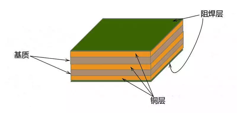
The solder mask is an indispensable component in the manufacture of printed circuit boards, serving primarily to shield metallic components on the board from environmental corrosion, particularly oxidation, while effectively preventing unintended electrical short circuits between pads, known as bridging. During soldering processes such as reflow or wave soldering, where precise control of solder placement proves challenging, the soldermask provides critical control. This layer is sometimes referred to as ‘solder resist’, a more appropriate term to avoid confusion with the overall solder layer covering the circuit board.
Types of PCB Solder Mask
Soldermasks comprise polymer layers applied over the metallic conductors of printed circuit boards. Selecting the most suitable soldermask type requires balancing cost-effectiveness with specific application requirements. The most fundamental application method employs screen printing to deposit liquid epoxy resin onto conductors. Soldermasks can be produced in various colours, with green being the most common, though red, blue, black, white, and yellow are also available.
Liquid Epoxy Soldermask
Liquid epoxy solder mask represents the most fundamental and economical option for PCB soldermasking. It involves applying liquid epoxy resin onto the PCB via screen printing. This printing technique utilises a woven mesh as a support to form a blocking pattern, allowing ink to pass through open areas. Liquid epoxy resin is a thermosetting polymer that gradually hardens during the thermal curing process. Manufacturers typically incorporate dyes into the liquid epoxy to achieve customised soldermask colours.
Liquid Photo-Stable Mask (LPSM)
More advanced soldermask techniques employ photolithography processes on dry film or liquid soldermask materials, operating similarly to photoresist exposure in semiconductor manufacturing. LPSM (also termed LPI) may be applied via screen printing or spraying. Spraying is generally the more cost-effective application method. The photolithography process enables more precise definition of soldermask openings around pads, vias, and mounting holes.
In practice, photomasks matching the desired soldermask pattern are fabricated from Gerber files. Prior to LPSM application, the PCB panel undergoes thorough cleaning to ensure no dust or contaminants remain beneath the cured solder mask. Subsequently, LPSM is applied to fully coat both sides of the PCB. LPSM material is UV-sensitive. After coating and drying, the board is placed in a UV developer. The black areas of the photomask define regions where conductors require exposure, while transparent areas preserve areas needing soldermask coverage. Upon UV exposure, the exposed LPSM material cures, while unexposed areas are solvent-washed away, ultimately forming a rigid soldermask layer. LPSM is available in multiple colours, such as green, black, red, yellow, white, and blue.
Dry Film Solder Mask (DFSM)
The process flow for Dry Film Solder Mask (DFSM) is similar to LPSM, also involving a photolithographic exposure process. Unlike liquid coating, the dry film is applied as a solder mask film via a vacuum lamination process. This vacuum lamination step ensures the unexposed soldermask adheres tightly to the PCB and effectively removes air bubbles within the film. Following exposure, solvents remove unexposed sections of the mask, after which the remaining film undergoes thermal curing.
Top and Bottom Layer Masks
Certain guides on PCB solder mask types frequently mention top and bottom layer masks. These terms simply denote masks applied to the top or bottom surface of the circuit board respectively, rather than denoting specific manufacturing processes or mask material types.
Solder Mask Process Flow and Surface Treatment
The soldermask process is often oversimplified by novices as ‘applying green mask → drying’, yet the complete procedure comprises six core steps: ‘pre-treatment → coating → pre-baking → exposure → development → curing’. Each stage influences the final properties of the solder mask, such as adhesion and resolution.
Pre-treatment
The purpose of pre-treatment is to remove grease, oxidation layers, and impurities from the PCB surface, ensuring the soldermask adheres tightly to both the substrate and copper layers to prevent subsequent peeling. This step typically involves degreasing, micro-etching, and drying. Degreasing employs ultrasonic cleaning with alkaline degreasers to remove oils, validated via water film testing. Micro-etching treats the copper surface with ammonium persulphate solution to create a roughened surface enhancing adhesion, typically controlled at 1-1.5μm depth. Finally, hot-air drying removes moisture to prevent bubbling during coating.
Coating
The purpose of coating is to uniformly cover the PCB surface with solder resist material, typically controlled at 10-30μm thickness, adjusted according to requirements. During operation, a 400-500 mesh screen (600 mesh for fine lines) may be used, with squeegee pressure of 0.2-0.3MPa and speed of 50-100mm/s to ensure even coating. Spraying employs a 0.5mm diameter nozzle at 0.15MPa pressure, maintaining a 15-20cm distance from the PCB surface for uniform application. This process must occur within a dust-free environment (Class 1000) to prevent particulate contamination.
Pre-baking
Pre-baking evaporates solvents (e.g., xylene) within the solder mask, transforming it from liquid to semi-solid state to prevent adhesion during subsequent exposure. Pre-baking typically occurs at 70–80°C for 20–30 minutes, with duration adjusted according to solder mask thickness. The pre-baked solder mask should feel tack-free to the touch without flaking, with residual solvent content below 1%.
Exposure
Exposure constitutes the critical step in forming the solder mask pattern. Ultraviolet light cures the exposed areas of the photosensitive solder mask, while unexposed regions (such as pads) are subsequently removed during development. During this process, the film bearing the solder mask pattern must be precisely aligned with the PCB, typically with a deviation of less than 0.05mm. Liquid photosensitive solder masks generally require 80-120mJ/cm² of energy, with an exposure time of 10-20 seconds.
Development
Development involves using a developer solution to dissolve the unexposed soldermask, thereby exposing the pads and areas requiring soldering. The commonly used developer is a 1%-2% sodium carbonate solution maintained at 30-35°C. Development typically lasts 60-90 seconds, followed by a 3-5 minute rinse with deionised water to remove residual developer. Post-development, the opened areas should be free of soldermask residue, with smooth pad surfaces, while the solder mask in non-opened areas should remain intact without peeling.
Curing and Surface Treatment
Following application of the aforementioned media, the circuit board requires thorough cleaning to eliminate all dust particles. Subsequently, the board undergoes final hardening and curing processes. Liquid epoxy solder mask layers are cured thermally. LPSM and DFSM films, however, are cured during photolithography via ultraviolet exposure, followed by thermal treatment to achieve further solidification and hardening. Curing temperatures typically range from 150-160°C for 60-90 minutes, with staged temperature increases to prevent solder mask cracking.
Regardless of the PCB solder mask type employed, the final layer invariably leaves certain copper areas exposed on the circuit board. These exposed regions must be plated with an appropriate surface finish to prevent oxidation. The most prevalent surface finish is Hot Air Solder Leveling (HASL). Additionally, Electrolytic Nickel Immersion Gold (ENIG) and Electrolytic Nickel Palladium Immersion Gold (ENEPIG) are commonly employed. Where applicable, additional apertures are reserved within the film layer for solder paste application, facilitating connection to pads or other components, and processed according to manufacturing requirements. One PCB surface treatment method involves simultaneously applying electroless nickel-gold plating to the gold fingers and solder pads, followed by applying blue moulding compound to the PCB, then applying electroplated thick gold to the gold fingers.
Standard Solder Mask Thickness
The thickness of the solder mask primarily depends on the thickness of the copper traces on the circuit board. In blank areas, the thickness of LPSM and DFSM solder masks may vary depending on location. Typically, the initial thickness of the solder mask is 0.5 mils. According to IPC standards, the minimum thickness for Class 2 products is 10μm, while Class 3 products require a minimum thickness of 18μm.
Typically, the average thickness in blank areas is approximately 10–18μm. Near conductor edges, the solder mask thins, potentially reaching 0.3 mils or less. Approximately 0.5 mils of solder mask coverage is generally required over traces. Sprayed epoxy solder mask facilitates more uniform thickness across the entire PCB. The solder mask not only prevents copper trace corrosion but also establishes barriers between adjacent pads. For component pads, this is achieved by defining a small gap (termed solder mask relief) between the mask and the exposed pad. This helps prevent solder bridging, proving particularly critical for high-density components such as fine-pitch BGAs. This design ensures solder can fully wet the pad and secure the component in place.
As a critical component in PCB manufacturing, the solder mask’s diverse types and precision manufacturing processes collectively ensure circuit reliability and stability. With the continuous evolution of electronic technology, ongoing innovations in solder mask technology will continue to provide vital support for high-performance, high-density electronic products.