Overview and Definition of Alumina Substrate PCBs
In the electronics manufacturing industry, with the continuous increase in device power density and increasingly stringent heat dissipation requirements, traditional epoxy resin fiberglass substrates (such as FR-4) are gradually failing to meet the demands of certain high-end applications. Against this backdrop, aluminum substrate PCBs (alumina substrate circuit boards), with alumina (Al₂O₃) as their core material, have emerged. Alumina substrate PCBs, a specialized circuit carrier based on a high-purity ceramic material, offer significant advantages in high-temperature resistance, insulation, mechanical strength, and heat dissipation. Consequently, they are widely used in demanding applications such as power modules, LED lighting, automotive electronics, RF microwaves, and aerospace.
Essentially, an aluminum substrate PCB is a composite structure with a conductive circuit layer formed on an alumina ceramic substrate. The ceramic layer serves as an insulating and supporting layer, while the metal layer facilitates signal transmission and heat dissipation. Depending on the manufacturing process and application requirements, this type of circuit board can be produced using processes such as thick film printing, thin film deposition, or direct bonded copper (DBC). DBC alumina substrate is currently the most representative form. It directly bonds the copper and ceramic layers through a high-temperature oxidation reaction, forming a monolithic structure with extremely strong adhesion and excellent thermal conductivity.
Alumina, as a base material, offers high hardness, high insulation resistance, low dielectric loss, and stable chemical properties. These properties enable it to maintain reliable electrical and mechanical performance even in extreme operating environments. Compared to other common ceramic materials (such as aluminum nitride (AlN) or silicon nitride (Si₃N₄), alumina’s greatest advantages lie in cost control and material processability. Although its thermal conductivity is slightly lower than that of aluminum nitride, Alumina Substrate PCBs still provide adequate thermal management capabilities in most mid-power applications while significantly reducing overall manufacturing costs.
Historically, the use of alumina ceramics as an electronic material dates back to the mid-20th century, when they were primarily used as substrates for vacuum tubes, sensors, and high-frequency circuits. With the continuous advancement of integrated circuits and power devices, engineers began exploring how to form finer and more reliable circuit patterns on ceramic substrates, driving the industrialization of ceramic circuit boards. Since the 21st century, with the explosive development of new energy vehicles, 5G communications, and high-brightness LED technology, the demand for high-heat dissipation and high-reliability PCBs has increased dramatically. Alumina Substrate PCBs have gradually become an indispensable carrier in high-end electronic packaging.
From an application perspective, the value of this type of ceramic substrate lies not only in its high-temperature resistance and excellent thermal conductivity, but also in its ability to effectively improve the overall power density and stability of the system. For example, in power modules, alumina substrates can directly serve as a transition layer between the chip and the heat sink, significantly reducing thermal resistance and extending device life. In high-frequency RF modules, their low dielectric constant contributes to accurate signal transmission and low loss.
In summary, Alumina Substrate PCBs are a circuit carrier solution that combines high performance with high reliability. It not only achieves an excellent balance of thermal, electrical, and mechanical properties, but also has gained widespread industrial application through its cost-effectiveness and mature manufacturing process. With the continuous evolution of electronic technology, this ceramic-based PCB is gradually moving from a “specialty material” to a “mainstream choice,” and will play an increasingly critical role in the future high-power, high-frequency, and high-stability fields.
Material Properties and Advantages of Alumina Substrate PCBs
The core advantages of Alumina Substrate PCBs (alumina substrate circuit boards) stem from their unique physical, chemical, and electrical properties. Alumina (Al₂O₃), a polycrystalline ceramic formed by high-temperature sintering, boasts a stable crystal structure and extremely high intermolecular bonding energy, enabling it to maintain excellent mechanical strength and chemical inertness even in extreme environments. It is not only resistant to humidity, oxidation, and most chemical corrosion, but also maintains structural stability at temperatures exceeding 1000°C. This property is extremely valuable for electronic systems that require extremely high environmental adaptability.
In terms of thermal performance, alumina has a high thermal conductivity, typically between 20 and 30 W/m·K. While lower than the 170-200 W/m·K of aluminum nitride (AlN), its heat dissipation capacity is dozens of times greater than the 0.3-0.4 W/m·K of traditional FR-4 materials. This means that in high-heat applications such as power modules, LED drivers, and radar systems, Alumina Substrate PCBs can quickly transfer heat generated by the chip to the heat sink, reducing junction temperatures and significantly extending device life and improving operational stability.
In terms of electrical properties, alumina has extremely high insulation resistance (typically exceeding 10¹⁴ Ω·cm), a low and stable dielectric constant (approximately 9.5), and extremely low dielectric loss. These properties make it an ideal carrier for high-frequency, high-voltage circuits. In particular, in RF microwave communication equipment, power converters, and automotive inverter systems, Alumina Substrate PCBs ensure low signal loss and interference during transmission, improving overall system energy efficiency and reliability.
Mechanical strength is also a key advantage of alumina. Its flexural strength can reach 300-400 MPa, and its hardness approaches Mohs 9, second only to corundum and diamond. Compared to metal or organic substrates, alumina ceramics offer significant advantages in dimensional stability, thermal expansion matching, and vibration resistance. In particular, its coefficient of thermal expansion (CTE) is approximately 6-8 ppm/°C, close to that of silicon chips (approximately 4 ppm/°C). This effectively prevents solder joint fatigue or cracking caused by thermal stress differences during the packaging process.
In terms of chemical stability and environmental adaptability, alumina exhibits excellent resistance to acids, alkalis, and most organic solvents, making it resistant to chemical reactions and degradation. This allows Alumina Substrate PCBs to maintain reliable operation over extended periods in harsh environments such as high humidity, salt spray, and high radiation. Consequently, they are widely used in applications requiring long-term stability, such as aerospace, military radar, and automotive electronic systems.
In addition, alumina’s surface smoothness and machinability facilitate circuit fabrication. After precision grinding and surface treatment, alumina ceramics can achieve submicron flatness, laying a solid foundation for processes such as metallization, welding, and thin-film deposition. Its surface roughness can be adjusted as needed, ensuring a balanced balance between conductive layer adhesion and signal transmission performance. Compared to other ceramics, alumina exhibits higher consistency and yield in processes such as laser drilling, screen printing, and thick-film sintering, making it considered the most mature and cost-effective solution for ceramic-based circuit boards.
Overall, the advantage of aluminum substrate PCBs lies in their balance between performance and cost. Although aluminum nitride (ANI) offers superior thermal conductivity, it is expensive and difficult to process. Metal-based PCBs, while dissipating heat quickly, suffer from insufficient insulation and are heavy. Alumina substrates, on the other hand, achieve a balance of high insulation, high strength, and moderate thermal conductivity at a relatively low cost, making them the preferred choice for many medium- and high-power electronic devices.
For this reason, alumina substrates strike an ideal balance between technical and economical performance, making them suitable not only for large-scale industrial production but also for maintaining excellent performance stability in specialized high-end electronic products. Whether addressing the thermal management challenges of power devices or the transmission requirements of high-frequency signals, Alumina Substrate PCBs stand out with their comprehensive performance, becoming a key support foundation for modern electronic systems.
Alumina Substrate PCB Manufacturing Process and Technology Route
The manufacturing process for Alumina Substrate PCBs (alumina substrate circuit boards) combines ceramic material engineering with microelectronics processing technology, resulting in a complex and precise process. Unlike traditional organic substrates, it requires high temperature, high pressure, and strict cleanroom conditions to ensure material density, electrical performance, and metal layer adhesion. The entire manufacturing process can be divided into four core steps: substrate preparation, metallization, circuit formation, and post-processing. Each step directly determines the thermal conductivity, insulation properties, and mechanical stability of the finished product.
In the substrate preparation stage, high-purity alumina powder (typically between 96% and 99.6% purity) is selected. After ball milling, granulation, and pressing, it is sintered at high temperature to form a ceramic green body. This process requires strict control of particle distribution and sintering temperature to achieve a dense and uniform grain structure. High-purity alumina can significantly improve dielectric properties and mechanical strength. However, even slight variations in sintering temperature and time can lead to substrate warping or porosity defects. To improve flatness and dimensional accuracy, finished substrates often undergo double-sided grinding and polishing to achieve micron-level thickness tolerances.
The metallization process is a key step in aluminum substrate PCB manufacturing. Depending on the application requirements, it can be categorized into three main technology routes: thick-film printing, thin-film deposition, and direct copper coating (DBC).
Thick-film printing technology applies metal paste (such as silver, palladium-silver, or gold) to the ceramic surface via screen printing, followed by high-temperature sintering to securely bond it to the substrate. This process is cost-effective and suitable for applications with wider circuit lines and a high concentration of power devices.
Thin-film deposition uses sputtering or evaporation to form an extremely thin metal layer on the alumina surface. Photolithography and etching are then used to create fine circuits. This method enables high-density wiring and excellent electrical performance, but is complex and costly, and is primarily used in RF and microwave modules.
DBC technology is currently the most representative and widely used process. It utilizes an oxidation reaction mechanism to form a strong interfacial layer between copper and alumina via Cu-O-Al chemical bonds at temperatures of approximately 1065°C. This process achieves excellent thermal conductivity and mechanical strength, making it suitable for high-power, high-reliability electronic modules.
During the circuit formation stage, different metallization methods correspond to different circuit manufacturing processes. For example, after the copper layer is bonded, chemical etching or laser cutting is performed to form the desired circuit pattern. To ensure etching accuracy and edge smoothness, photosensitive dry film and precision exposure equipment are typically used to control line width tolerances within ±20μm. Thick-film printed circuits achieve multi-layer interconnects through multiple printing layers and precise sintering. Thin-film circuits rely on plasma etching and vacuum deposition techniques to form nanoscale conductive layers.
Post-processing includes through-hole fabrication, surface plating, pad protection, and final cutting and forming. Due to the extremely high hardness of alumina ceramics, traditional mechanical drilling is inefficient and prone to damage, so laser drilling is more commonly used. Through-hole metallization can be achieved through electroless copper or palladium-nickel deposition, ensuring electrical interconnection between multiple layers. Common surface treatments include gold plating, silver plating, and OSP to enhance solderability and oxidation resistance. Finally, the circuit board is cut into individual pieces to meet the designed dimensions through precision cutting or CNC machining.
The entire manufacturing process requires extremely high equipment precision, cleanliness, and thermal control. Even the slightest deviation can lead to quality issues such as warping, cracking, or metal layer delamination. To ensure consistency and reliability, manufacturers often incorporate automated optical inspection (AOI), X-ray inspection, and microstructural analysis into production to monitor the material bonding state at every stage.
It is worth noting that with the advancement of power electronics and packaging technology, new process routes are constantly evolving. For example, active metal brazing (AMB) technology uses an active metal interlayer (such as titanium or zirconium) to strengthen the bond between copper and aluminum oxide, further improving thermal cycling resistance. Thick copper plating and multilayer ceramic lamination technologies provide greater design freedom for high-current and high-density wiring. These process innovations have enabled Alumina Substrate PCBs to gradually transition from single-layer structures to multi-layer and composite structures, opening up new possibilities for high-power modules and integrated packaging.
Overall, the manufacturing process for Alumina Substrate PCBs is a systems engineering effort that spans materials science and microelectronics technology. It requires not only a deep understanding of the physical properties of the ceramic substrate but also a high degree of control over processes such as metallization, etching, and soldering. It is precisely this precision process and multidisciplinary integration that has ensured the long-term stability, reliability, and mass production of Alumina Substrate in the electronics manufacturing industry.
Typical Applications of Alumina Substrate PCBs
The fundamental reason Alumina Substrate PCBs hold a prominent position among numerous circuit carrier materials is their excellent insulation properties, superior thermal conductivity, and exceptional mechanical strength, enabling them to excel in a variety of high-power, high-temperature, and high-reliability scenarios. With the increasing complexity of electronic systems, increasing power density, and the continued advancement of miniaturized packaging, Alumina Substrate PCBs are gradually penetrating multiple key industries.
First, power electronics modules are one of the most widely used applications for aluminum substrate PCBs. Power devices generate significant heat during operation. Failure to dissipate heat quickly can lead to elevated junction temperatures, impacting device lifespan and performance. While the thermal conductivity of aluminum oxide substrates is lower than that of aluminum nitride, it far exceeds that of standard FR-4 substrates, making it sufficient to meet the heat dissipation requirements of medium- and high-power modules. For example, in IGBT modules, MOSFET drivers, and DC/DC converters, aluminum oxide substrates often serve as an intermediate layer between the chip and the heat sink. This not only ensures electrical insulation but also provides an efficient heat conduction path, significantly improving overall system stability and energy efficiency.
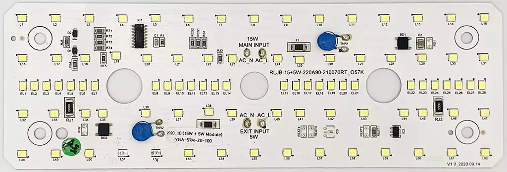
Second, aluminum substrate PCBs also play a key role in the LED lighting and display sectors. With the widespread adoption of high-brightness LEDs, chip overheating has become an increasingly prominent issue. Using aluminum oxide substrates can effectively reduce LED junction temperatures, improve luminous efficacy and color temperature consistency, and extend device lifespan. Aluminum oxide substrates, particularly in automotive headlights, tunnel lighting, outdoor advertising screens, and high-power projectors, have become a mainstream choice due to their excellent heat dissipation and weather resistance. In addition, its high reflectivity and excellent dimensional stability facilitate optical design and assembly.
In automotive electronic systems, Alumina Substrate PCBs are widely used in power control units (PCUs), on-board chargers (OBCs), inverter modules, and sensor systems due to their high-temperature resistance, vibration resistance, and high dielectric strength. New energy vehicles are particularly dependent on this high-reliability substrate to ensure the safe operation of electric drive systems in high-temperature and high-humidity environments. Compared to metal substrates, Alumina substrates offer superior stability during thermal cycling and can withstand the structural stresses caused by frequent starts and stops and thermal shock, making them highly favored in automotive-grade products.
In RF and microwave communication equipment, Alumina Substrate PCBs’ low dielectric constant and extremely low dielectric loss make them an ideal carrier for high-frequency signal transmission. They effectively reduce signal attenuation and crosstalk, maintaining transmission stability and accuracy. In particular, in radar modules, RF filters, antenna arrays, and the RF front-end of 5G base stations, alumina substrates, with their excellent electrical properties and dimensional stability, ensure reliable system operation at high frequencies. Furthermore, their high surface flatness enables more precise circuit routing, meeting the packaging requirements of highly integrated modules.
Sensors and measurement and control devices are also key applications for Alumina Substrate PCBs. Many temperature, pressure, and humidity sensors must operate in harsh environments, such as high temperatures, corrosion, or strong radiation. Alumina ceramic’s excellent chemical stability and electrical insulation ensure the long-term reliability of these devices. Furthermore, the low thermal expansion properties of ceramic substrates help improve the measurement accuracy and response consistency of sensor elements, leading to their widespread use in industrial control, petrochemical, medical testing, and aerospace test systems.
Furthermore, in the aerospace and defense electronics sector, alumina substrates’ high strength, radiation resistance, and low failure rate make them a crucial component of critical electronic modules. They can be found in radar systems, power conditioning units, navigation control modules, and satellite communications equipment. Their excellent vacuum resistance and stable thermal performance ensure the continued operation of electronic systems in environments with extreme temperature fluctuations, strong vibration, and high radiation.
In recent years, with technological advancements, medical electronic devices have also begun to adopt alumina substrate PCBs extensively. Applications such as ultrasound probes, heart rate monitors, and implantable electronic devices all have stringent requirements for electrical insulation, thermal stability, and biocompatibility. Alumina ceramics, due to their non-toxic, non-magnetic, and corrosion-resistant properties, are ideal packaging and support materials. Furthermore, their precision machinability facilitates the development of smaller and more precise medical electronic modules.
Overall, the application areas of aluminum substrate PCBs cover virtually all electronic systems with high performance, reliability, and heat dissipation requirements. It is not only a core material for power modules and LED packaging, but is also gradually expanding into strategic industries such as new energy, RF communications, high-end medical, and military electronics. As device power increases and packaging integration increases, the advantages of aluminum oxide substrates will become increasingly prominent, making them an indispensable foundational material in future electronics manufacturing.
Future Trends and Development Directions of Alumina Substrate PCBs
With the continuous evolution of the electronics industry and the continuous increase in system integration, the development of aluminum substrate PCBs (alumina substrate circuit boards) is moving towards higher performance, greater precision, and greater sustainability. Although alumina ceramic materials have achieved considerable performance, their manufacturing processes, material systems, and structural designs continue to innovate in demanding applications such as next-generation power electronics, RF communications, and new energy vehicles. Future development trends can be explored from the following perspectives.
First, from the perspective of material optimization and composite technology, while the thermal conductivity of traditional aluminum oxide ceramics meets most applications, it remains insufficient for high-power modules and high-speed packaging. Therefore, research institutions and manufacturers are working to improve thermal conductivity through material modification. For example, introducing boron nitride, silicon carbide, or metal oxide nanofillers into an alumina matrix can enhance heat dissipation efficiency while maintaining high insulation properties. Furthermore, the development of composite ceramic materials allows alumina to be combined with other ceramic materials, such as aluminum nitride and zirconium oxide, to form multifunctional composite structures through co-firing or lamination, achieving a balance of thermal conductivity, electrical insulation, and mechanical strength. This optimization of material systems will enable aluminum substrate PCBs to achieve new breakthroughs in performance and cost.
Secondly, in terms of manufacturing process and structural innovation, ceramic circuit boards are evolving from single-layer to multi-layer and integrated. While traditional single-layer alumina substrates are stable and reliable, multi-layer ceramic PCBs (such as LTCC and HTCC structures) are emerging as device miniaturization and system integration increase. Through low- or high-temperature co-firing processes, conductors, impedance matching networks, and heat conduction channels can be embedded between ceramic layers, creating a three-dimensional interconnect structure. This not only increases circuit density and signal integrity but also provides more flexible packaging options for complex electronic systems. At the same time, the introduction of next-generation laser micromachining and precision photolithography processes has enabled alumina substrates to achieve ever-increasing control over trace widths, via dimensions, and metal layer adhesion.
In terms of surface metallization and interconnect technologies, traditional thick-film printing and DBC processes are being gradually supplemented by higher-performance AMB (active metal brazing) and DPC (direct copper plating) technologies. AMB uses active brazing filler metals (containing active elements such as titanium or zirconium) to improve the metal-ceramic interface bond quality, maintaining a stable bond even under extreme thermal cycles. DPC utilizes laser imaging and electroless copper plating to form a fine copper layer on the ceramic surface, offering excellent adhesion and resolution, making it ideal for high-precision circuit fabrication in the RF and microwave fields. These advanced metallization processes will drive the continued expansion of alumina substrates in high-frequency, high-power, and high-reliability applications.
Furthermore, heat dissipation structures and system integration design will also become important development areas. With chip power density continuing to increase, relying solely on material thermal conductivity is no longer sufficient to meet demand. In the future, aluminum substrate PCBs may be combined with metal heat sinks, liquid cooling structures, or graphene thermal conductive layers to create efficient composite heat dissipation systems. Integrating thermal channels or microfluidic cooling structures within the substrate can further improve heat dissipation efficiency and reduce system temperature rise. Furthermore, module-level packaging technologies (such as SiP and 3D packaging) will drive ceramic substrates towards system integration, making them not only circuit carriers but also core components of functional modules.
In terms of green manufacturing and sustainable development, with tightening global environmental regulations, energy consumption and waste disposal in the aluminum substrate PCB production process have become key industry concerns. Future manufacturing will increasingly utilize low-energy sintering, recycled slurry systems, and reusable process water recycling solutions to reduce the environmental impact of production. Furthermore, research is underway into the recycling of ceramic materials, such as mechanical pulverization and chemical separation to regenerate alumina powder for secondary sintering or filler materials. This circular manufacturing model not only meets environmental requirements but also reduces overall production costs.
Based on industry application trends, aluminum substrate PCBs will be deeply integrated with emerging fields in the future. With the rapid development of new energy vehicles, 5G communications, artificial intelligence, and renewable energy, the demand for high-power, high-frequency, and high-reliability substrates will continue to grow. Alumina substrates, with their mature process and high cost-effectiveness, will remain a key supporting material for mid- to high-end electronics manufacturing. Furthermore, in devices operating under extreme conditions, such as satellite electronics, aerospace propulsion systems, and deep-sea exploration instruments, alumina’s chemical inertness and mechanical toughness will ensure their long-term competitiveness.
Overall, the future direction of Alumina Substrate PCBs is the parallel development of performance and intelligent manufacturing. On the one hand, continuous innovation in materials engineering and micromachining technologies will achieve higher thermal conductivity, stronger bonding strength, and superior electrical performance. On the other hand, automated production and AI-powered inspection systems will improve yield and consistency, driving ceramic-based PCB production towards larger-scale, higher-precision, and more intelligent models.
Conclusion
In summary, Alumina Substrate PCBs, as the most mature, stable, and cost-effective solution in the ceramic PCB system, have established a core position in power electronics, LED lighting, automotive electronics, RF communications, and other fields with their superior thermal, electrical, and mechanical properties. It’s not just a connection and heat dissipation carrier; it’s the foundation for the reliable operation of electronic systems. With continuous breakthroughs in new materials and processes, alumina substrates are evolving from a single carrier structure to a high-performance composite substrate, moving from traditional manufacturing to intelligent and green production. In the future, they will continue to play an irreplaceable role in the core links of the electronics industry, providing solid support for high-end manufacturing and technological innovation.
