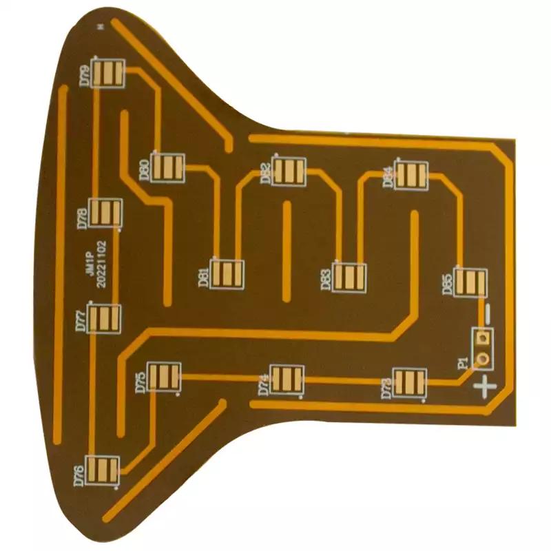
The design of flexible printed circuits (FPC) is a complex and intricate process that requires consideration not only of the flexibility demands of the application scenario but also of multiple technical factors to ensure product reliability and manufacturing feasibility. This guide aims to detail the key considerations in flexible board design and provide effective strategies to mitigate potential manufacturing issues during the design phase, thereby achieving efficient and high-quality product development.
Design Steps and Key Considerations
Application Requirements Level
Within the flexible circuit board design process, the primary task is to define appropriate flexibility requirements based on the actual application scenario. Some flexible printed circuits may only require basic non-coplanar connections, bending just once during installation. Conversely, flexible circuits in hinges for flip phones endure repeated bending cycles. The most demanding applications, such as those for hard disk drive heads, require flexible circuits capable of sustained, repetitive bending motions. Given the varying bending requirements across different scenarios, designers must select the most suitable solution.
Installation Methods
Common interconnection approaches between flexible and rigid boards include:
Board-to-board connectors: The most prevalent method, encompassing surface-mount, through-hole, and crimp types. Note that this approach necessitates reinforcing plates for the flexible printed circuits, resulting in increased overall height post-assembly. Both connector costs and assembly expenses remain substantial.
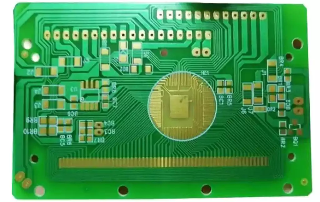
Connectors with gold fingers: This method enhances interconnection density and typically offers a slimmer profile, though it demands high precision in gold finger fabrication.
Hotbars: Although requiring specialised assembly equipment, their application scope is gradually expanding.
When selecting a specific mounting method, comprehensive consideration must be given to factors such as interconnection height, effective area, connector cost, and processing expenses. Additionally, different interconnection methods impose varying requirements on manufacturing precision.
Layer Stackup and Shielding
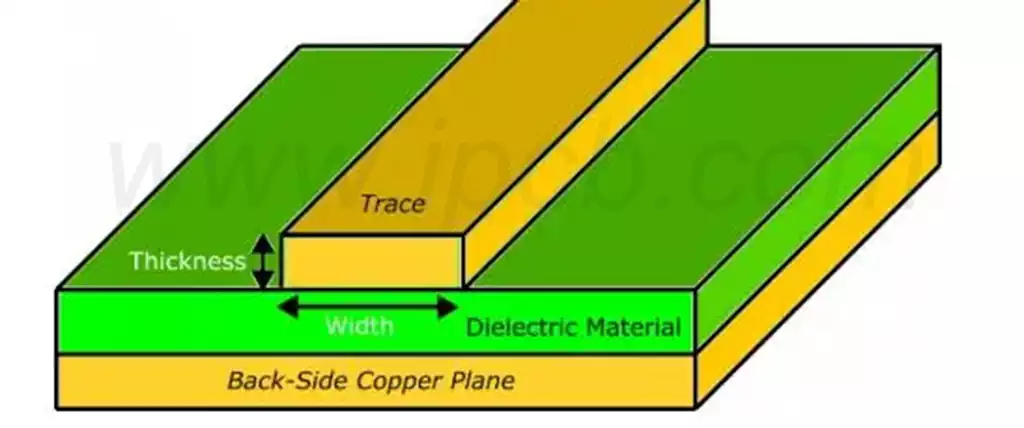
Layer Design: Common stackup configurations in flexible circuit board design include single-sided, double-sided, and double-sided with silver paste layers. When impedance control is required, designers may flexibly combine these structures to form microstrip or stripline traces.
Shielding Control: For electromagnetic interference (EMI) mitigation, shielding layers can be incorporated. Shielding layer types include solid copper foil, copper foil mesh, and silver paste mesh. Solid copper foil is the most common shielding method, applicable to one side, both sides, or even just the specific areas requiring shielding. However, solid copper foil increases the number of layers in the FPC, thereby complicating the manufacturing process.
Timing Analysis and Signal Quality Aspects
During the flexible circuit board design phase, timing analysis becomes particularly crucial when trace lengths exceed certain thresholds. This analysis primarily evaluates the impact of trace delay on signal transmission. Additionally, attention must be paid to potential signal attenuation and distortion during transmission. To address these issues, techniques such as driving, matching, or equalisation may be employed to ensure signal quality.
Conductive Capacity Aspect
Accurate assessment of the current-carrying capacity for signals is indispensable during flexible circuit board design. Both trace width and copper cladding thickness must meet specific current-carrying requirements with adequate margin. Particular attention must be paid to high-current lines such as power and ground traces, meticulously planning connector pin counts, trace quantities, and widths.
Environmental Compliance
On 27 January 2003, the European Union formally issued the RoHS Directive (Restriction of Hazardous Substances), restricting the use of toxic materials in relevant products. Manufacturers were mandated to comply from 1 July 2006. For flexible printed circuit (FPC) design, particular emphasis is placed on ensuring substrates contain no halogen components.

How to Avoid Manufacturing Issues During the Design Phase of Flexible Circuit Boards
Many problems encountered in flexible board manufacturing can actually be prevented during the design stage.
- Allow for Bending Radius
Do not permit sharp right-angle bends in traces; use arcs or gradual curves instead.
For single-layer PI boards, the bending radius should be ≥5–10 times the board thickness.
For multilayer boards, increase the bending radius further to avoid stress concentration. - Avoid Routing in Repeatedly Bent Areas
Refrain from routing traces in frequently folded zones.
If routing is unavoidable, trace in the same direction and avoid crossings.
Placing vias or components in flexible bend zones is not recommended.
- Optimal Structural Layout
Offset via areas from bend zones to prevent crack propagation.
Add reinforcement structures (e.g., cover plates or thickened PI) on both sides of pads.
When employing gold fingers or ZIF connectors, reinforce the gold finger area additionally.
- Consider panelisation for fabrication
Flexible circuit boards should not be manufactured as single pieces; panelisation must be planned.
Support fabrication using FR4 auxiliary frames or rigid carrier sheets.
Positioning holes should be reserved on the process edge to facilitate subsequent placement and testing.
Flexible printed circuits design requires comprehensive consideration across multiple dimensions. By meticulously planning bend radii, trace routing, structural integrity, and panelisation during the design phase, manufacturing challenges can be effectively mitigated, enhancing product reliability and production efficiency. Continuous attention to design details and close collaboration with manufacturing are key to achieving outstanding product performance.


