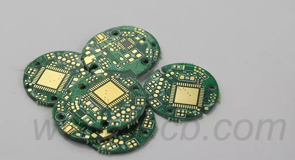
PCB blistering refers to localised swelling or bulging occurring within or on the surface of printed circuit boards (PCBs) during production or use. This phenomenon typically manifests as separation between the substrate and copper foil, solder mask, or other layers, forming bubbles or voids.
Causes of PCB Blistering
Substrate Processing Issues
Particularly concerning thinner substrates (generally below 0.8mm), their reduced rigidity makes brush cleaning unsuitable. This may fail to effectively remove protective coatings applied during substrate manufacturing to prevent copper foil oxidation. Production processes must therefore be carefully controlled to prevent poor adhesion between the substrate copper foil and electrolytic copper plating, which can cause surface blistering.
Surface Processing Issues
Contamination from oils or other liquids adhering to the surface during machining operations (drilling, laminating, edge milling, etc.), or dust contamination.
Poor copper plating on etched boards
Excessive pressure during pre-etching grinding deforms hole edges, resulting in rounded copper foil corners or even exposed substrate at the hole perimeter. This causes blistering around holes during immersion copper plating, tin spraying, and soldering processes. Therefore, rigorous control of the etching process is essential. Optimal etching parameters can be achieved through scratch tests and water film tests.
Rinsing Issues
As electroless copper plating involves extensive chemical treatment, inadequate rinsing of the board surface—particularly when adjusting degreasers for copper plating—not only causes cross-contamination but also leads to localised treatment failures or suboptimal results. Therefore, rigorous control of the washing process is essential, primarily encompassing the regulation of water flow rate, water quality, washing duration, and the drip time of the boards.
Electroless Copper Plating Issues
Micro-etching during the pre-treatment for electroless copper plating and the pre-treatment for pattern plating. Excessive micro-etching may expose the substrate at the hole opening, causing blistering around the aperture. Insufficient micro-etching can also result in inadequate adhesion, triggering blistering. Therefore, micro-etching control must be enhanced. Typically, the micro-etching depth for pre-treatment before electroless copper plating ranges from 1.5 to 2 micrometres, while that for pattern plating pre-treatment is between 0.3 and 1 micrometre. Where feasible, micro-etching thickness or rate should ideally be controlled through chemical analysis and simple weighing tests.
Oxidation Issues
Oxidation occurs on the board surface during production. For instance, oxidation of electroplated copper boards in air may not only result in copper-free holes and a rough board surface but also cause surface blistering. Therefore, electroplated copper boards should undergo timely thickening treatment during production and should not be stored for extended periods.
Poor Re-work of Electroplated Copper
Substandard re-work on electroplated copper or post-pattern transfer boards may cause surface blistering due to inadequate stripping, incorrect re-work methods, improper micro-etching time control, or other factors. If electroplating defects are detected during online re-work, boards may be re-worked directly after washing and degreasing without micro-etching; re-degreasing and micro-etching should be avoided where possible.
Oxidation of board surfaces during production
If electroplated copper boards oxidise in air, this may not only cause copper-free holes and surface roughness but also lead to blistering. Prolonged storage in acid baths can also cause oxidation, forming a film that is difficult to remove.
Management of pickling tanks prior to copper plating
Contaminated baths and elevated copper concentrations adversely affect panel cleanliness. Pickling tanks require timely replacement to prevent excessive contamination or high copper levels, which not only compromise surface cleanliness but also induce defects such as surface roughness.
Organic contamination in electroplating tanks
Oil residues within electroplating tanks necessitate regular cleaning to ensure panel quality. Particularly prevalent in automated production lines, oil contamination necessitates regular cleaning of electroplating tanks to maintain cleanliness, thereby safeguarding PCB board quality and performance.
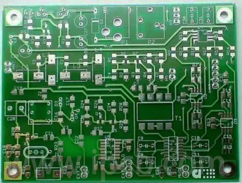
To prevent PCB blistering, manufacturers may implement the following measures:
- Strictly control the production environment, ensuring temperature and humidity remain within appropriate ranges;
- Utilise high-quality raw materials and ensure their storage conditions are optimal;
- Rigorously implement cleaning procedures to ensure complete solvent evaporation and thorough rinsing;
- Optimise process parameters to avoid excessive heating temperatures and prolonged heating durations;
- Conduct regular equipment inspections to guarantee uniform pressure and balanced force distribution during lamination.
- Re-evacuation: For PCB boards exhibiting blistering, re-evacuation may be employed for remediation. This method enhances copper foil adhesion by eliminating residual air between the foil and substrate. Temperature and pressure must be carefully controlled during repair to prevent further damage to the PCB board.
- Heat baking: Heat baking is a common method for resolving copper foil bubbling on PCBs. By baking the PCB board at a specific temperature, adhesion between the copper foil and substrate is enhanced, preventing bubble formation. This method is straightforward to implement and yields noticeable results. However, temperature and duration must be strictly controlled during baking to avoid overheating or scorching the PCB board.
PCB blistering not only compromise circuit board performance and reliability but may also lead to resource wastage and increased production costs. By thoroughly analysing the causes of bubbling and implementing targeted preventive and remedial measures, manufacturers can effectively reduce the occurrence of bubbling problems, thereby enhancing PCB quality and production efficiency. Only through rigorous control of every stage in the production process can the stability and reliability of the final product be ensured, meeting market demands for high-quality circuit boards.
