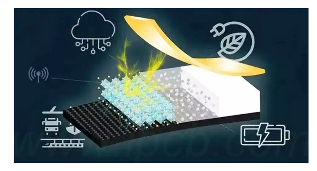
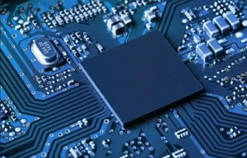
AI server PCBs serve as the core electronic components within artificial intelligence servers, connecting and supporting critical elements such as processors, memory, accelerators, and power management systems. They enable high-speed signal transmission, high-power-density power delivery, and efficient thermal management to meet the demands of AI computing for large-scale data processing and high-speed operations.
Amidst the intensifying competition for AI computing power, five critical types of PCBs within AI servers—featuring up to 44 layers and necessitating specialised M9 materials—are increasingly becoming the foundational hardware supporting the training of large models like ChatGPT.
As the race for AI computing power grows fiercer, industry focus is shifting from the quantity of GPUs to the more fundamental choice of PCB materials. Within high-end AI server cabinets, five critical PCB boards—computing boards, switching boards, CPX boards, mid-boards, and backplanes—collectively form the hardware foundation for training trillion-parameter models.
The performance of these PCB materials directly impacts data transmission speeds, signal integrity, and system stability. Material selection has become a pivotal factor influencing AI computational efficiency, with the application of advanced materials representing a core competitive advantage in AI server design.
Five Key PCB Boards: The “Neural Hub” of AI Servers
The intricate internal structure of an AI server cabinet resembles a sophisticated neural system, where these five PCB boards each fulfil distinct roles while operating in concert. The compute board, as the core component, handles GPU/TPU computational tasks; the switch board facilitates high-speed data exchange between boards; and the CPX board undertakes specialised computational acceleration functions.
The mid-board plays a crucial connecting role within AI servers, linking compute boards and CPX boards to ensure high-speed data flow. The confirmed 44-layer construction of the mid-board fully reflects its exceptional complexity. To meet high-speed signal transmission demands, the mid-board must utilise M9 material, paired with Q-step quartz cloth and fourth-generation copper foil.
The backplane, serving as the foundational platform for the entire system, provides stable power distribution and fundamental signal connectivity for the server. Both the CPX board and backplane are confirmed to utilise M9 or higher-grade materials to guarantee baseline system performance.
The most critical material selections for the compute board and switch board are anticipated to be finalised by late 2025. Current mainstream projections suggest the compute board may adopt M8 material, while the switch board could potentially utilise M9 material.
The Path to Material Advancement: Performance Leap from M8 to M9
Selecting PCB materials for AI servers is far from a simple comparison of specifications; it is a systematic engineering endeavour encompassing signal integrity, thermal management, and long-term reliability. As a premium choice, M9 material offers distinctly superior performance.
M9 material meets the high-performance demands of servers, with its primary advantages lying in lower dielectric loss and a more stable dielectric constant. For 44-layer mid-boards, employing M9 ensures high-speed signals traverse complex transmission paths without severe distortion or attenuation.
AI server PCBs require high-layer counts and high-density interconnect (HDI) capabilities, supporting manufacturing processes for 16 to 40 layers or more. M9 material excels in high-end manufacturing, accommodating board thicknesses exceeding 3mm and aspect ratios greater than 15:1.
In contrast, M8 material offers slightly diminished performance but lower cost, potentially making it more suitable for cost-sensitive applications such as compute boards. For switch boards handling high-speed signal switching tasks, the likelihood of employing M9 material continues to increase over time.
AI servers generate substantial heat during continuous operation, necessitating PCBs with high thermal conductivity (exceeding 3W/m·K). Uniform copper plating and optimised heat dissipation hole designs are also essential to ensure long-term stable server operation. High thermal density has become one of the primary challenges for AI server PCBs.
Thermal management issues become increasingly complex as PCB layer counts rise. Take a 44-layer mid-board as an example: it necessitates advanced thermal management techniques, such as thermal via fillers, to enhance thermal equilibrium by optimising heat dissipation pathways.
AI server PCBs demand stringent thermal resistance and low coefficient of thermal expansion (CTE), requiring high heat resistance (glass transition temperature Tg exceeding 170°C) and low CTE to prevent deformation in high-temperature environments. M9 material excels in these properties, withstanding the sustained thermal stress induced by AI training workloads.
For high-power zones, embedded copper coining technology significantly enhances thermal dissipation. Additionally, uniform electroplated copper thickness (no less than 25μm) is critical, ensuring high current-carrying capacity and preventing failure due to overheating.
Manufacturing Challenges: The High Barriers to Precision Production of High-End PCBs
The manufacturing requirements for AI server PCBs are exceptionally stringent. The 44-layer core board must utilise M9 material (paired with Q-step quartz cloth and fourth-generation copper foil), as only M9 can meet the high-performance demands of servers. High-layer PCB manufacturing involves precise lamination and drilling processes.
PCBs demand exceptional flatness; for surface-mount applications, maximum warpage and twist must not exceed 0.75%. Achieving this standard for 44-layer thick boards necessitates advanced lamination techniques and appropriate material selection.
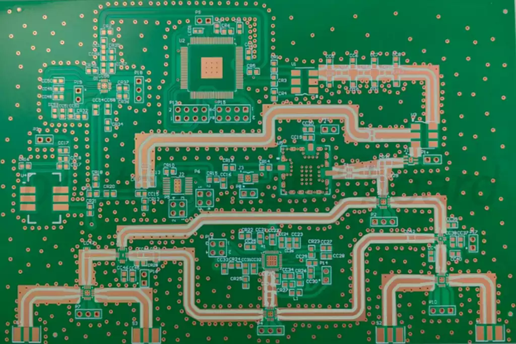
Drilling with aspect ratios of 15:1 or greater demands extreme precision. Laser micro-blind via technology aids in reducing parasitic inductance, enhancing high-speed signal integrity. Line width/spacing must reach 0.09/0.09mm or smaller, necessitating high-precision imaging and etching techniques. Impedance control accuracy must achieve ±5% to accommodate high-speed protocols such as PCIe 5.0/6.0, 100G/400G Ethernet, and DDR5. Automated impedance testing (TDR) combined with SI simulation optimisation is a critical measure to ensure PCBs meet high-speed computing demands.
Driven by both material upgrades and process refinements, AI server PCBs are continually pushing performance boundaries, laying a robust foundation for the sustained advancement of AI computing power.