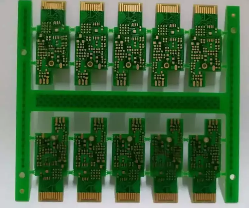
The optical module PCBA manufacturing process involves assembling optoelectronic devices and electronic components onto printed circuit boards. Through a series of processing steps, this manufacturing technique enables the conversion and transmission of optical signals into electrical signals.
In optical module PCBA production, the surface mount technology (SMT) process demands exceptionally high placement accuracy. For components such as 0201-sized resistors and capacitors, placement deviation must be controlled within ±0.05mm to ensure reliable electrical connections.
With the rapid advancement of 5G, data centres, and high-speed optical communications, optical modules—as core transmission components—face increasingly stringent performance and reliability requirements. Within optical module PCBA processing, the COB process is widely adopted due to its high integration and cost-effectiveness, while fibre coupling precision stands as a critical determinant of module performance.
The Relationship Between COB Process and Fibre Coupling Precision
The COB process involves directly packaging optical chips onto a PCB substrate to achieve the conversion between optical and electrical signals. During this process, the coupling precision between the fibre end-face and the optical chip directly impacts the transmission efficiency and stability of optical signals. If coupling deviation exceeds ±1μm, it may significantly increase optical power loss or even cause communication interruptions. Therefore, controlling coupling precision necessitates coordinated optimisation across materials, processes, and equipment.
Key Control Points in PCBA Processing
During PCBA processing, focus should be placed on the following aspects to support precision control in subsequent COB processes:
Substrate Design and Material Selection
The flatness of the PCB substrate (typically requiring warpage below 0.1%) and its thermal expansion coefficient must be compatible with the optical chip. This prevents deformation during high-temperature soldering or curing, which could cause fibre displacement.
Precision Assurance in SMT Placement
Employ high-precision SMT placement machines (e.g., with placement accuracy within ±25μm) to ensure accurate positioning of driver circuit components. This prevents pad misalignment from affecting the optical chip’s positioning reference.
Solder Paste Printing and Reflow Soldering Management
Optimising stencil aperture design and reflow temperature profiles minimises solder splatter or bridging, preventing contamination of the optical chip mounting area.
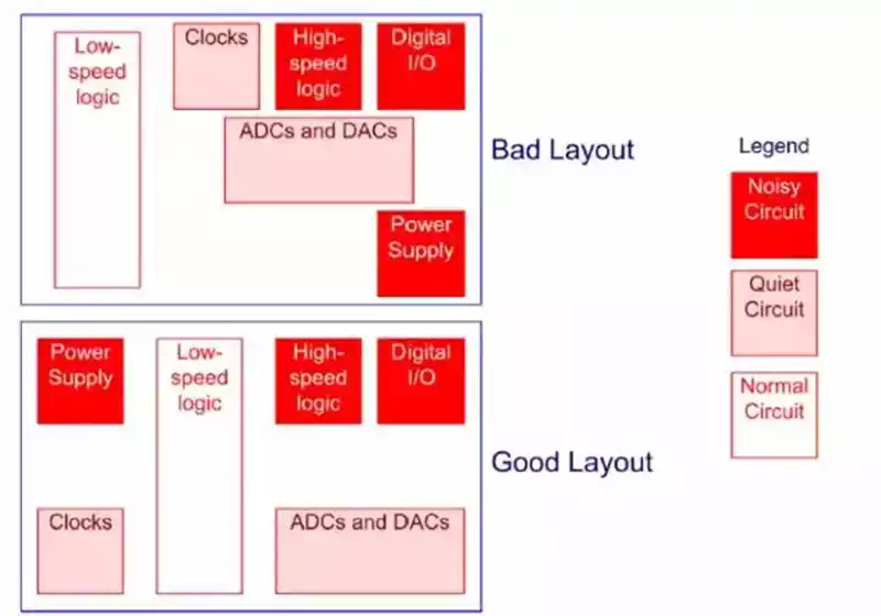
During reflow soldering, differing melting points of solder pastes (e.g., common SnAgCu paste at approximately 217°C) necessitate strict control of the reflow profile, typically with a heating rate of 1-3°C/s. In wave soldering for optical module PCBA manufacturing, the wave height is typically controlled at approximately two-thirds of the printed circuit board thickness. This ensures full solder joint coverage and minimises cold solder joints. The fabrication of the circuit board’s solder resist layer is critical; its thickness generally ranges between 25–40μm. An appropriate thickness prevents issues such as solder bridging. For high-speed signal traces in optical modules, routing should maintain a minimum spacing of 1.5 times the trace width to minimise signal interference.
During cleaning processes, solvents must effectively remove flux residues and contaminants. Water-based cleaners are typically maintained at a pH value between 7 and 9. During the testing phase of optical module PCBA, optical performance tests require transmit optical power accuracy of ±0.5 dBm to ensure stable optical signal output. Component layout must maintain a minimum distance of 10 mm between optoelectronic devices and other heat-generating components to prevent thermal degradation of optoelectronic performance. In screen printing, character clarity and adhesion are critical. Screen printing inks are typically dried at temperatures between 80-100°C, with a drying time of approximately 15-30 minutes.
When assembling optical module housings, screw tightening torque is specified. For commonly used M3 screws, for instance, tightening torque is controlled between 0.5-0.8 N·m to prevent housing loosening that could compromise performance.
Control Measures for Fibre Coupling in COB Processes
High-Precision Positioning and Die Attach Processes
Active Calibration Technology: Utilising a vision alignment system (e.g., CCD camera) in conjunction with a six-axis micro-adjustment platform to perform real-time calibration of positional deviations between the optical chip and fibre end-face. Following calibration, an optical power monitoring feedback system must verify whether the coupling efficiency meets specifications.
Optimisation of Adhesive Curing Parameters: Select UV or epoxy adhesives with low shrinkage rates. Employ staged temperature control during curing (e.g., gradually heating from 25°C to 80°C) to prevent fibre displacement caused by adhesive contraction.
Synergistic Optimisation of SMT and COB Processes
Component Layout Design: During SMT placement, reserve operational space for COB processes to prevent peripheral components (e.g., capacitors, inductors) from obstructing visual calibration paths or interfering with dispensing operations.
Equipment Compatibility Management: Standardise coordinate systems across SMT production lines and COB equipment to ensure seamless alignment between placement coordinates and optical chip positioning coordinates, thereby minimising errors from secondary calibration.
Inspection and Feedback Mechanisms
Online Monitoring Technology: Integrate real-time optical power detection modules within the COB process. These modules shall collaborate with AOI (Automated Optical Inspection) equipment to analyse the morphology and intensity of coupled light spots. Parameters shall be adjusted promptly based on analysis outcomes.
Environmental Control: Establish a constant temperature and humidity workshop, maintaining temperatures at 23±1°C and humidity between 40%–60%. This mitigates thermal expansion and contraction effects on PCBA substrates and optical fibres, ensuring long-term stability.
Optical module PCBA manufacturing involves intricate and complex processes where each stage is intricately linked. Precise control over critical elements is essential to forge high-performance products, thereby propelling the flourishing development of the optical communications industry.