PCB impedance control technology for optical modules pcb is central to ensuring signal integrity in high-speed optical communication modules. Its key lies in precisely controlling the physical parameters of transmission lines on printed circuit boards (such as line width and dielectric thickness) through meticulous design and manufacturing processes, enabling precise impedance matching with system requirements (typically 100 ohms differential impedance). This approach aims to minimise signal reflection and loss, thereby guaranteeing stable and reliable data transmission at 400G, 1.6T, and even higher data rates.
Why Impedance Control is Central to High-Speed Optical Module PCB Design
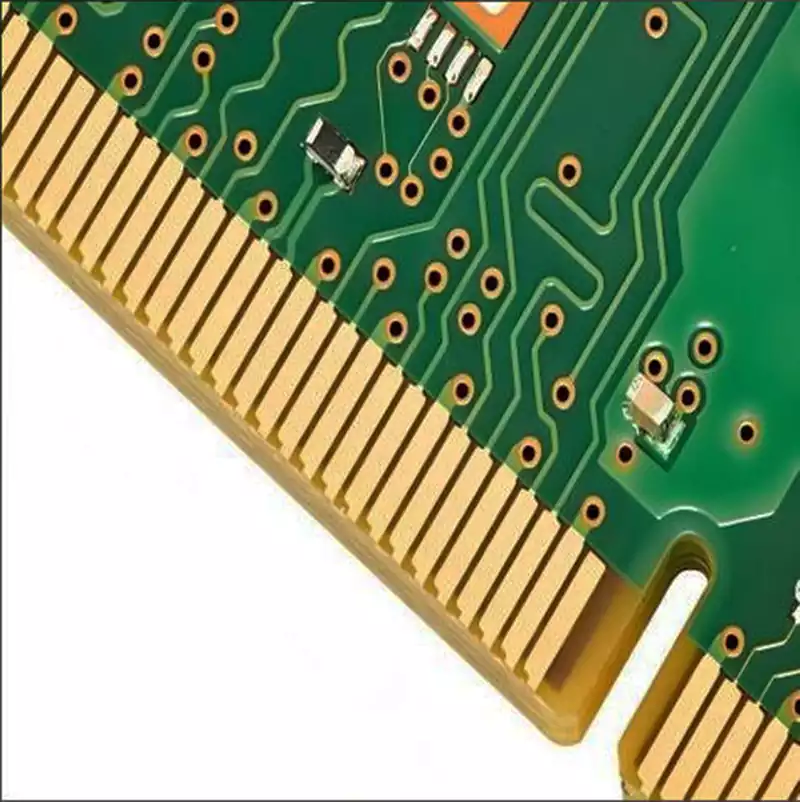
In the realm of high-speed digital signals, traces on printed circuit boards (PCBs) are not mere connecting wires but must be treated as transmission lines. When signal frequencies reach the gigahertz (GHz) range, subtle physical effects become dramatically amplified. As the hub for optoelectronic conversion and high-speed data transmission, optical modules operate at extremely high internal signal rates where even minute signal distortion can cause communication failure. Precise impedance control thus forms the cornerstone of design, its importance chiefly manifested in safeguarding ‘signal integrity’.
Signal Integrity (SI) denotes a signal’s capacity to maintain its quality throughout its transmission path. When signals traverse PCB traces, mismatched characteristic impedance between the transmission line and the source or receiving end can induce reflection phenomena akin to light striking a mirror. A portion of the signal energy reflects back to the source, superimposing on the original signal and causing severe waveform distortion such as overshoot and ringing. This distortion compresses the eye pattern’s aperture used to distinguish data ‘0’s and ‘1’s, ultimately leading to a sharp increase in the Bit Error Rate (BER). This significantly compromises the performance and reliability of optical modules.
For ultra-high-speed optical modules such as 400G and 1.6T, the data transmission rate implies extremely short bit periods for each signal. Within such a brief timeframe, even microsecond-level signal reflections and delays are sufficient to interfere with subsequent data interpretation. Therefore, the impedance of PCB traces must be strictly controlled within an extremely narrow tolerance range (e.g., ±8% or even ±5%) to ensure signal energy is transmitted smoothly and maximally from transmitter to receiver. It can be said that without rigorous impedance control, the performance of high-speed optical modules is unattainable, which is also one of the key reasons for their complex design and high cost.
Key Technical Factors and Parameters Affecting the Impedance of Optical Module PCBs
Achieving precise impedance control fundamentally involves the meticulous calibration of PCB physical parameters and material properties. Designers must coordinate multiple variables like a conductor orchestrating a symphony to produce a harmonious ‘impedance composition’. The factors influencing PCB characteristic impedance are intricate, but can primarily be categorised into three main groups: conductor geometry, dielectric properties, and manufacturing process tolerances.
Firstly, conductor geometry is the decisive factor. This encompasses trace width, thickness (copper thickness), and distance from the reference plane (typically ground or power planes). According to an analysis by Bora Circuit, trace width is one of the most direct influences on impedance: wider traces yield lower impedance, and vice versa. Similarly, increased copper thickness also reduces impedance. Therefore, during production, high-precision exposure and etching equipment must be employed to control line width tolerances within an extremely narrow range, such as within 10%, to establish the foundation for the final impedance accuracy.
Secondly, the properties of the dielectric are crucial. The dielectric layer—the insulating material between conductors and the reference plane—directly influences impedance values through its dielectric constant (Dk) and thickness. A lower dielectric constant or thicker dielectric layer results in higher impedance. In high-speed optical module PCBs, high-speed laminates (such as Rogers or Megtron series) with low dielectric constants and loss factors (Df) are typically selected to replace conventional FR-4 materials. This is because high-speed materials not only minimise signal energy loss but also exhibit greater stability in Dk values across varying frequencies and temperatures, thereby ensuring impedance consistency. Furthermore, controlling dielectric thickness during multilayer board lamination poses a significant challenge, as any deviation in thickness directly translates to impedance variation.
Ultimately, the precision of manufacturing processes determines whether theoretical designs can be successfully realised. Beyond trace width and dielectric thickness, the thickness of solder resist ink also influences the impedance of surface-layer traces, typically causing a slight impedance reduction. These intertwined factors impose exceptionally high demands on PCB manufacturers’ process capabilities.
Processes and Measurement Techniques for Achieving High-Precision Impedance Control
Accurately reproducing the ideal impedance values from design drawings onto physical PCBs constitutes a systematic endeavour integrating precision engineering with stringent process control. The core challenge lies in countering the inevitable variables and tolerances inherent in manufacturing. Achieving the ±5% impedance tolerance demanded by high-end optical modules requires not only advanced equipment but also rigorous monitoring of every potential error source throughout the production flow.
At the production process level, the first step involves raw material control. The dielectric constant and thickness of the substrate must fall within the supplier’s specified tolerances and undergo incoming material inspection. Secondly, during the pattern transfer stage, the use of a parallel light exposure machine enables more precise reproduction of the line widths from the master film compared to traditional point light sources, thereby reducing deviation. During lamination, advanced press technology ensures uniform flow of dielectric layers under high temperature and pressure, resulting in greater consistency in final dielectric thickness. Etching is the critical step for controlling line width; manufacturers must apply precise process compensation based on experience to counteract side etching effects, ensuring the final line width meets design specifications.
However, sophisticated manufacturing processes alone are insufficient; reliable measurement techniques are essential to validate the final outcome. Currently, the industry-recognised standard measurement method is the Time-Domain Reflectometer (TDR). As detailed in Huaqiu Circuit’s technical articles, TDR has become the established technique for measuring PCB characteristic impedance. TDR operates by transmitting a rapid step pulse signal along the transmission line under test (i.e., the impedance test strip on the PCB) while simultaneously monitoring the reflected waveform. If the impedance remains uniform and matched throughout the transmission line, no reflection occurs. Any variation in impedance generates a reflected signal. By analysing the amplitude and timing of these reflections, the TDR precisely calculates the impedance value at every point along the transmission line. This process resembles using echoes to map the structure of a cave.
To ensure TDR measurement accuracy, strict operational protocols must be followed. For instance, calibration using traceable standards is required prior to measurement. Test samples should be secured with specialised fixtures during testing to prevent external interference, and test probes and cables must be regularly inspected for wear. By fabricating impedance test coupons with identical structures to actual traces along the board edge during production and subsequently performing TDR testing post-manufacture, manufacturers can effectively verify whether the impedance control of entire PCB batches meets specifications. This provides reliable assurance for the performance of high-end optical modules.
PCB Design Strategies for 400G/1.6T and Future Optical Modules
As optical communication technology advances towards 400G, 1.6T and beyond, demands on PCB signal integrity have reached unprecedented levels. While traditional impedance control methods form the foundation, they are insufficient to address the complex challenges posed by ultra-high-speed signals, such as attenuation, crosstalk, and mode conversion. Consequently, designers must adopt a suite of more advanced and refined design strategies to ensure signal quality at the system level.
The first step involves further upgrading material selection. In the 1.6T era, signal frequencies are extremely high, making transmission loss a performance bottleneck as critical as impedance. Designers must select ultra-low loss or even extremely-low loss grade substrates. These materials not only exhibit lower and more stable Dk/Df values but also feature specially treated copper foil roughness to minimise skin effect and conductor loss during high-frequency signal transmission.
Secondly, at the layout level, more advanced signal integrity techniques are required. For instance, in the gold finger area of optical modules, achieving impedance matching proves exceptionally challenging due to complex connector structures. Some advanced designs employ a ‘segmented gold finger’ approach, grouping multiple pairs of high-speed differential lines and performing detailed simulation and optimisation of each segment’s geometry to ensure impedance continuity across the entire connection area. Furthermore, for traces beneath BGA (Ball Grid Array) packaged chips, designers employ ‘anti-pad’ techniques to prevent pad-induced impedance disruption. This involves etching out the corresponding BGA pad area on the reference plane layer, thereby controlling signal path impedance.
Finally, the application of simulation tools has become indispensable. During the design phase, engineers must employ specialised electromagnetic field simulation software (such as Ansys HFSS or Cadence Clarity) to perform precise 3D modelling and simulation of the entire signal chain, including vias, connectors, and packages. Through simulation, potential impedance discontinuities and signal integrity issues can be identified and optimised iteratively beforehand, rather than discovering problems only after prototypes are manufactured and tested. This ‘simulation-driven design’ approach significantly shortens the R&D cycle and increases the probability of first-time success, making it the essential choice for developing ultra-high-speed optical module PCBs.
Frequently Asked Questions (FAQ)
- Why are optical modules so expensive?
The high cost of optical modules directly reflects their technological complexity. Firstly, they integrate precision optical components such as lasers and detectors alongside high-speed modulation chips, all of which are inherently costly. Secondly, achieving ultra-high-speed data transmission at hundreds of Gbps or even Tbps necessitates exceptionally stringent PCB design and manufacturing. As discussed herein, this demands costly high-speed, low-loss materials alongside extremely precise impedance control and signal integrity design, substantially increasing fabrication costs. Finally, rigorous testing protocols, substantial R&D expenditure, and a relatively monopolistic market landscape further contribute to the high price point. - What is the operating temperature range for optical modules?
Optical modules are typically categorised by operating temperature range into commercial-grade and industrial-grade variants. Commercial-grade (COM) optical modules operate within 0°C to 70°C, primarily suited for temperature-controlled environments such as data centres. Industrial-grade (IND) optical modules, however, must operate stably within a broader range of -40°C to 85°C, making them suitable for harsh environments like outdoor base stations. It is worth noting that temperature variations affect the dielectric constant of PCB materials, leading to impedance drift. Consequently, industrial-grade optical modules demand higher stability in impedance control across the entire temperature spectrum. - What is the bandwidth of an optical module?
The ‘bandwidth’ of an optical module typically refers to its data transmission rate. Current market offerings span a broad range, from early 100Mb/s and 1Gb/s modules, to mainstream 10Gb/s, 25Gb/s, 40Gb/s, and 100Gb/s, to the 400Gb/s widely deployed in data centres and backbone networks, and the emerging 800Gb/s and 1.6Tb/s. Higher rates demand exponentially greater signal integrity, thereby presenting greater challenges for PCB impedance control techniques, material selection, and overall design.