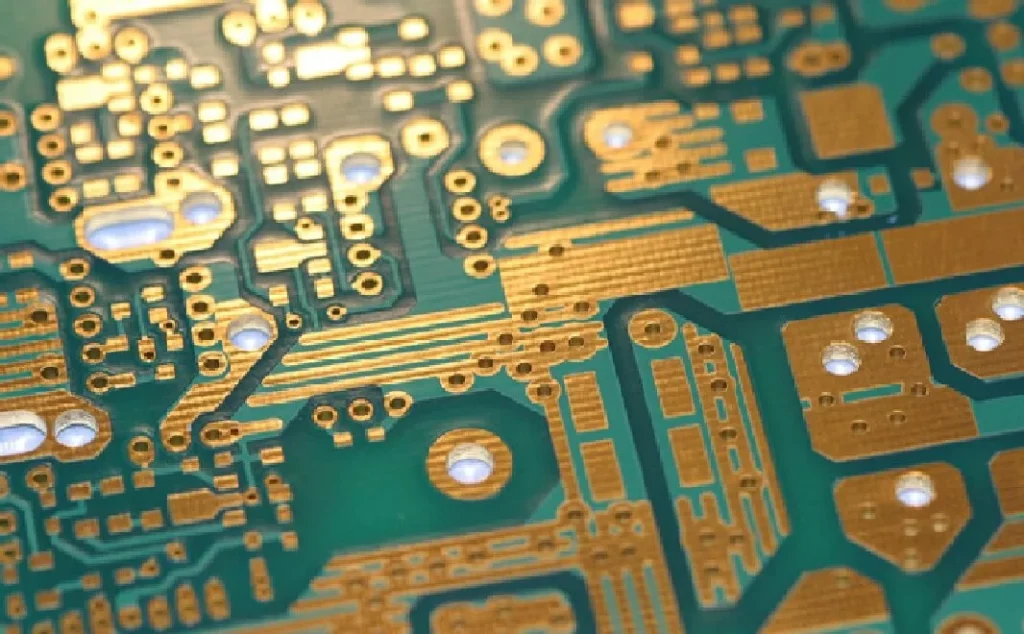
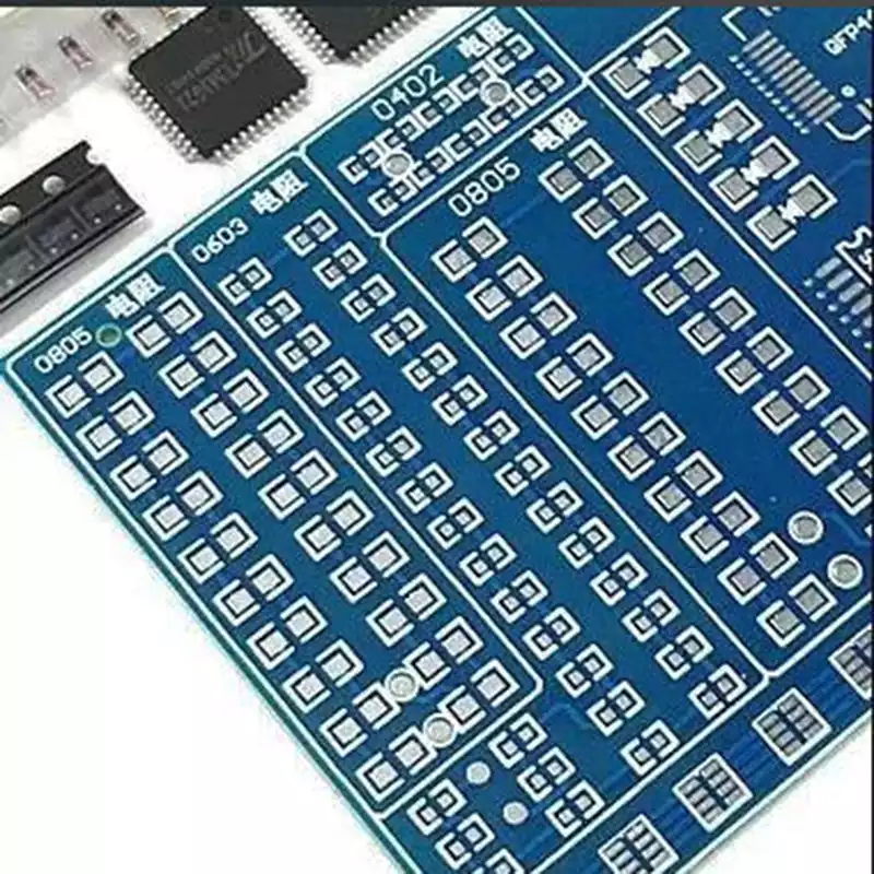
During the production or rework stages of PCB circuit boards, pcb pads are highly susceptible to damage, ranging from localised fractures to complete detachment from the substrate. Such damage directly compromises the reliable soldering of components, ultimately rendering the entire PCB inoperable and unusable.
The core value of pcb pad repair technology lies in its ability to precisely address localised defects, thereby preventing the scrapping of entire PCBs due to minor damage and significantly reducing production costs. However, it must be emphasised that all pcb pad repair operations must strictly adhere to process specifications. Improper repair techniques may instead introduce reliability hazards, potentially causing issues such as cold solder joints or poor contact during subsequent use.
Eight Common PCB Pad Repair Methods:
- Copper Foil Patch Method
For minor surface pad damage, copper foil patching offers a cost-effective and straightforward solution. Precisely cut micro-copper foil squares are applied over the affected area and cured with epoxy resin. Note that long-term reliability heavily depends on the epoxy’s bonding strength, making this suitable for temporary repairs in low-stress environments. - Copper Tape Patch Method
For wider pcb pad damage, conductive copper tape patches offer a more robust solution. Select copper tape of appropriate width to cover the damaged area, then encapsulate the outer layer with heat-resistant Kapton tape for insulation. This method significantly enhances peel resistance during rework by strengthening mechanical support, making it particularly suitable for repairing equipment in high-frequency vibration environments. - Circuit Frame Reinforcement Method
For scenarios requiring sealed repair materials, circuit frame technology achieves precise filling by constructing insulating barriers. A customised insulating frame is first bonded around the pad perimeter, followed by injection of conductive epoxy resin to complete the repair. This method overcomes dimensional constraints, enabling flexible repair of pads of any specification. The sealed structure effectively blocks moisture and contaminant ingress. - Conformal Coating Reconstruction Method
In densely populated areas with narrow pad spacing, conformal coating technology maximises space utilisation through layered application. An insulating acrylic coating first covers the damaged substrate, followed by a conductive layer to reconstruct the pad’s functional layer. This method is simple to operate, requiring no complex tools, and is particularly suitable for repairing minute pads in consumer electronics. - Solder Mask Bridging Repair Method
For partially detached pad segments, solder mask bridging restores electrical continuity by filling gaps with solder mask material. The process involves applying solder mask to bridge the break, followed by an electro-deposition technique to reconstruct the complete pad. This method preserves the original layout while delivering conductivity and mechanical strength comparable to the original pad. - Epoxy Resin Bonding Method
For pcb pads requiring preservation of their original geometry, conductive epoxy resin injection enables non-destructive repair. Precision injection equipment fills the cavity beneath the pad with resin, which cures to form a robust bond. This technique demands extensive operator expertise, as improper filling or trapped air bubbles may cause poor contact. - Jumper Bridge Method
For pin fractures with minute gaps, jumper bridging restores electrical continuity by soldering insulated fine wires. Enamelled wires under 0.1mm diameter span the break, with both ends soldered and reinforced by insulating adhesive. This method occupies minimal space but necessitates strict control of wire bending radius to prevent long-term stress-induced metal fatigue fractures. - Multilayer Board Rework Technology
For deep-seated damage in high-value multilayer PCBs, specialised rework techniques achieve precise repairs through layer-by-layer delamination. Surface cover films are first stripped to expose inner-layer pads, with the board’s layered structure reconstructed post-repair using original manufacturing processes. This method requires laser delamination equipment and X-ray positioning systems, being applicable solely to irreplaceable precision circuit boards in aerospace, medical devices, and similar sectors.
From simple surface-mount repairs to complex rework, these eight restoration techniques address the full spectrum of PCB pad damage scenarios. Practical implementation requires selecting solutions based on damage type, equipment value, and operational environment, while strictly adhering to cleanroom protocols.