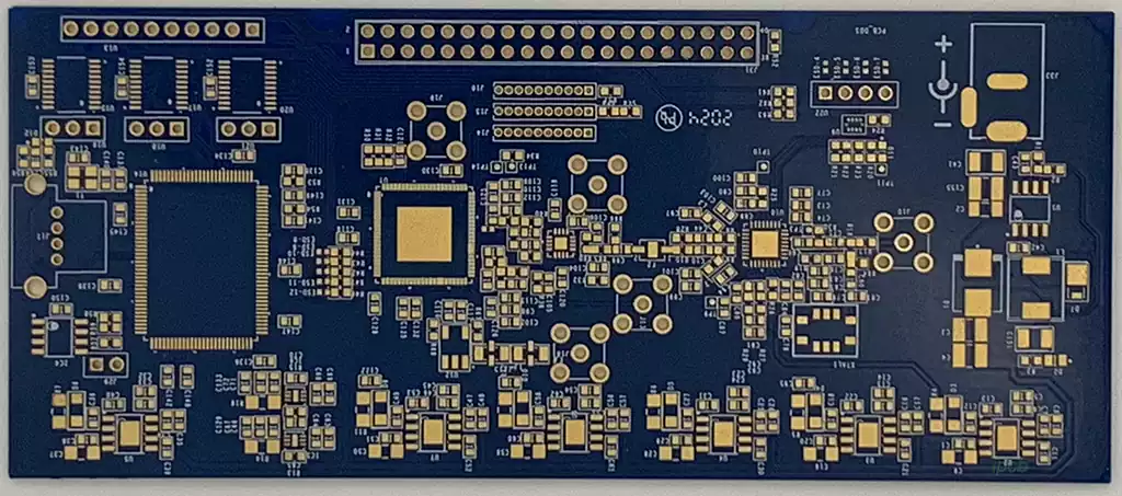
In traditional semiconductor packaging processes, lead frames serve as the conductive pathways for integrated circuits (ICs) while also functioning as the supporting substrate. The pins are connected to either the sides or the perimeter of the lead frame. However, as semiconductor packaging technology has advanced, conventional packaging formats such as QFP encountered limitations when pin counts exceeded 300.
Against this backdrop, novel semiconductor packaging formats such as BGA and CSP emerged in the mid-1990s. Concurrently, a new product emerged as a critical carrier for semiconductor chip packaging: the semiconductor package substrate (IC Package Substrate, also termed semiconductor packaging substrate).
The primary function of IC package substrates is to establish electrical connections (acting as a transition layer) between the chip and the different circuits on conventional printed circuit boards (mostly motherboards, backplanes, or mainboards). They also provide protection, support, and heat dissipation pathways for the chip, enabling it to meet standard mounting dimensions. These substrates offer numerous significant advantages, such as enabling multi-pin configurations, reducing the footprint of packaged products, improving electrical and thermal performance, and achieving high density. Consequently, semiconductor packaging substrates in forms such as BGA, CSP, and flip chip (FC) have seen rapid expansion in application domains and gained widespread popularity in recent years.
Given the extensive utilisation of high-density multilayer substrate technology in semiconductor packaging and the pressing need to reduce packaging substrate manufacturing costs (for BGA, substrate costs account for approximately 40%-50% of total costs; while for FC substrates it constitutes 70%-80% of the manufacturing cost), semiconductor packaging substrates have become a crucial ‘instrument’ for national and regional microelectronics industry development.
Classification of Semiconductor packagin Technologies
Packaging Technologies Incorporating Enclosures
Packaging methods employing traditional enclosures, alongside those utilising packaging substrates, are categorised together as packaging technologies utilising enclosures during the packaging process.
Embedded Packaging Technology
Embedded Component Packaging (ECP) differs significantly from most conventional packaging types. Typically, within numerous integrated circuit packaging forms, the device is positioned atop the substrate, which acts as a bridge connecting the device to the packaging board.
Bare Die Packaging and Wafer-Level Packaging (WLP) Technology
Secondary packaging primarily involves the packaging and assembly of printed circuit boards (PCBs), specifically the mounting of primary-packaged components onto PCBs. This process encompasses interconnections between on-board packaging units and devices, whilst also considering factors such as impedance control, trace fineness, and the application of low-dielectric-constant materials. Unless special requirements dictate otherwise, this level of packaging typically does not incorporate additional encapsulation bodies. Products such as computer graphics cards and PCI data acquisition cards fall within the scope of secondary packaging. Should this level of packaging achieve certain complete functionalities and require installation within a unified housing, examples include National Semiconductor’s USB data acquisition cards and Creative’s external USB sound cards.
Lead Frame Packaging Technology
Traditional semiconductor packaging employs lead frames as both conductive pathways and structural supports for the integrated circuit, with pins connected along the frame’s sides or perimeter. As IC packaging technology advances, increasing pin counts (exceeding 300 pins), denser line layouts, and greater substrate layer counts have imposed limitations on further development of conventional formats like QFP.
The technique employing conventional lead frames and encapsulation shells is termed lead frame packaging technology, predominantly applied in square flat no-lead packages (QFN) and quad flat package (QFP) domains.
Function of Leads in Lead Frame Packaging
Ensuring Superior Conductivity
Within lead frame packaging, the lead frame plays a pivotal role within the plastic encapsulation. It connects the chip’s functional elements to the external pins on the frame via leads, while integrated circuit chips often rely on leads to connect the chip’s ground lines to the frame base. Consequently, the lead frame must possess outstanding electrical conductivity to ensure stable and efficient current transmission, thereby guaranteeing proper chip operation.
Efficient Thermal Conductivity Facilitates Heat Dissipation
During operation, chips generate heat, particularly in high-power products where substantial operating currents produce greater thermal loads. This heat is primarily dissipated through the lead frame and moulded plastic. Inadequate thermal management risks chip damage from overheating. The PN junction is typically designed for a working temperature of 150°C. Excessive temperatures may cause thermal breakdown of the junction during operation. For high-power products, specific sections of the lead frame may incorporate dedicated heat sinks to enhance thermal dissipation capacity.
Good Thermal Expansion Matching for Temperature Adaptation
Within the plastic encapsulation, the lead frame is physically bonded to the chip via silver paste and directly contacts the moulding compound. During encapsulation, reflow soldering, and operation, all materials expand when heated. Therefore, excellent thermal expansion matching between different materials is essential to prevent issues arising from differential expansion and ensure the stability of the encapsulation structure.
Reliable Bond Strength to Counteract Thermal Stress
The lead frame connects to the chip via silver paste and comes into direct contact with the moulding compound. During production and operation, thermal exposure is unavoidable. Although thermal expansion between materials is optimised, residual thermal stress inevitably persists. Consequently, robust bonding strength between the lead frame and all materials is essential to withstand thermal stress and prevent separation or detachment.
Applications of Lead Frame Packaging
Lead frame packages such as SO, QFP, and QFN remain most prevalent in semiconductor products with fewer than 200 I/O pins. Their moulds typically employ wire bonding, featuring relatively straightforward packaging methods. However, packages incorporating flip-chip, multi-mould, and mould/passive component combinations are now also in volume production.
Current Status of Ceramic Packaging
Ceramic packaging may largely be regarded as a traditional technology. While once widely employed in the IC sector, it is now almost exclusively used in fields demanding exceptional reliability, such as military and avionics applications. These sectors, driven by stringent stability and reliability requirements, are reluctant to readily adopt changes in packaging technology.
Semiconductor packaging technology has evolved significantly over the years. From traditional lead frame packaging to the emergence of novel packaging forms, and the continuous refinement of various specialised techniques, each step has borne witness to the vigorous development of the microelectronics industry. Traditional lead frame packaging, with its simplicity and reliability, continues to hold an important position in specific fields. Novel packaging substrate technologies, responding to demands for multi-pin configurations and high density, have become key drivers of industrial progress. while embedded and bare die packaging technologies continue to excel in their respective specialised domains. Ceramic packaging, though increasingly confined to specific high-reliability applications, provides vital insights for the stable evolution of packaging technologies. Looking ahead, as technological advancements continue, semiconductor packaging will inevitably pursue sustained innovation. This will not only address increasingly diverse requirements but also propel the microelectronics industry towards new heights, injecting continuous momentum into global technological development.