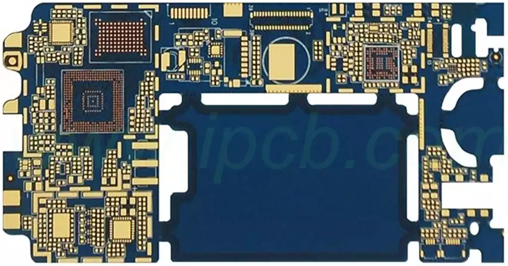
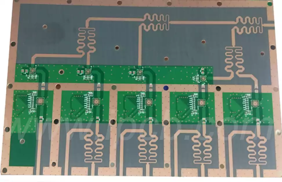
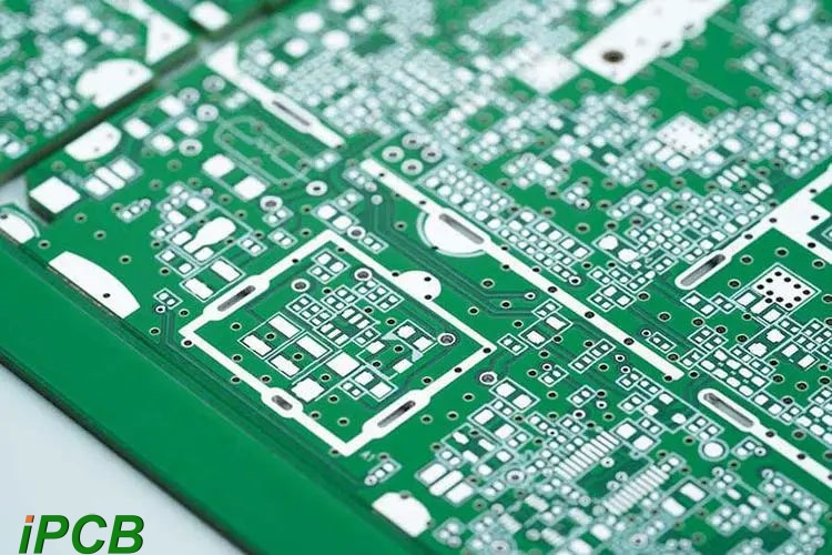
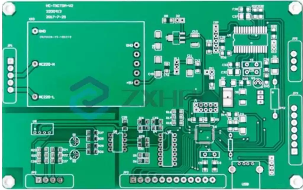
In the current era of continuous innovation in electronic technology and increasingly widespread application of high-frequency circuits, high-frequency hybrid boards have distinguished themselves in numerous circuit designs through their unique advantages. Not only do they excel in ensuring high-frequency signal transmission quality and precisely controlling impedance, but they also play a vital role in cost control, meeting complex design requirements, and adapting to specialised environmental applications. Simultaneously, the calculation and reduction strategies for hybrid board trace losses represent a critical aspect in enhancing circuit performance.
Advantages of High-Frequency Hybrid Boards
Enhancing High-Frequency Signal Integrity
Within high-frequency circuits, signal transmission speed and quality are paramount. High-frequency hybrid-pressure technology employs high-frequency laminates with low dielectric constant (Dk) and low dielectric loss factor (Df) in signal layers, effectively reducing delay, distortion, and attenuation during signal propagation. Take GHz-level high-speed digital signals or high-frequency analogue signals, such as RF signals in 5G communications or high-speed data transmission lines in data centres, as examples. High-frequency hybrid PCBs ensure signals maintain excellent integrity during interlayer transmission, minimising signal reflection and crosstalk. This consequently enhances the overall performance and reliability of the circuit system.
Enhanced Impedance Control Precision
Different high-frequency laminates possess specific parameters such as dielectric constant and thickness, enabling more precise control over layer impedance in high-frequency hybrid pcb design. By judiciously combining high-frequency materials with standard materials and meticulously designing trace widths, spacing, and layer thicknesses, precise impedance matching can be achieved for diverse signal paths, fulfilling 50Ω or other specific impedance requirements. Precise impedance control minimises energy loss during signal transmission, further enhancing transmission efficiency and quality. This is particularly advantageous for circuits demanding stringent impedance matching, such as RF front-end circuits and high-speed differential signal transmission lines.
Achieving Cost-Effectiveness Balance
Targeted Material Selection Reduces Costs
Although high-frequency laminates offer outstanding electrical performance, they typically carry a higher cost. High-frequency hybrid-press technology permits the use of high-frequency materials solely on critical signal layers, while employing cost-effective standard FR-4 material for power planes, ground planes, or low-speed signal layers where electrical performance requirements are relatively lower. This targeted material application effectively reduces material costs while ensuring the entire PCB meets high-frequency circuit design requirements. For instance, in PCB designs for mass-produced consumer electronics like smartphones and tablets, high-frequency hybrid-press technology optimises the performance of high-frequency functional sections (such as Wi-Fi and Bluetooth wireless communication modules) without significantly increasing costs, thereby enhancing product cost-effectiveness and market competitiveness.
Enhancing Yield and Manufacturability
High-frequency hybrid-press technology partially accommodates the overall manufacturability of PCB boards. Given the widespread adoption of FR-4 material within the PCB manufacturing industry, its mature processing techniques yield high production yields. Combining high-frequency materials with FR-4 leverages the processing convenience of FR-4 to reduce overall PCB manufacturing complexity, thereby mitigating increased scrap rates caused by intricate processing methods. For instance, during multilayer PCB lamination, FR-4 material parameters are relatively straightforward to control. When combined with high-frequency materials, this ensures high-frequency layer performance while enhancing lamination process stability and success rates. Consequently, production efficiency increases and manufacturing costs decrease.
Meeting Complex Design Demands
Flexible Functional Zoning in Multilayer Structures
PCB designs for modern electronic devices grow increasingly intricate, often requiring multiple functionalities to be integrated onto a single board. High-frequency hybrid lamination technology offers greater flexibility for functional zoning in multilayer PCBs through the combination of different material laminates. For instance, in a complex PCB design incorporating high-speed digital circuits, RF circuits, and analogue circuits, this technology enables optimised design for high-speed digital signal layers and RF signal layers separately. Analogue circuit layers can then be tailored with appropriate materials and design approaches based on their specific characteristics. This flexible functional partitioning allows the PCB to better meet requirements for electrical isolation, signal transmission, and grounding between different circuit modules, thereby enhancing PCB integration and system performance.
Adaptation to Special Environments and Applications
In specialised applications such as aerospace, military communications, and industrial automation control, PCBs must not only exhibit excellent high-frequency performance but also meet specific environmental adaptability requirements. High-frequency hybrid-press technology combines high-frequency materials with properties like high-temperature resistance, chemical corrosion resistance, and high mechanical strength with standard FR-4 materials, enabling PCBs to function reliably under harsh environmental conditions. For instance, in aerospace electronics, PCBs may encounter extreme conditions including high temperatures, intense radiation, and severe vibration. Employing high-frequency hybrid-lamination technology—combining high-temperature-resistant, highly reliable high-frequency laminates with FR-4—ensures long-term stable operation in complex environments, meeting the stringent requirements of aerospace systems for electronic equipment.
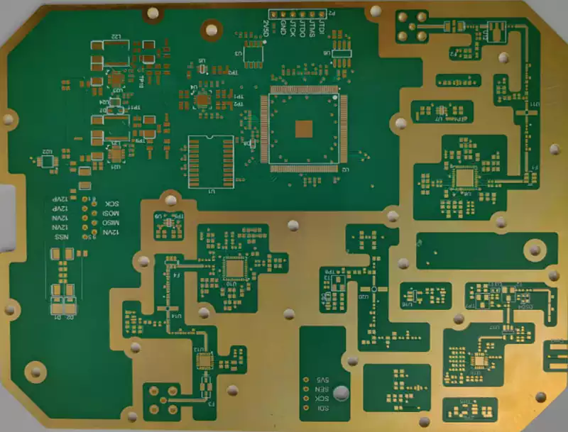
Calculation Method for Trace Losses in Hybrid Boards
Definition of Trace Losses
Generally speaking, trace losses refer to the energy dissipation incurred when current flows through conductors on a pcb board. This loss arises from factors such as the conductor’s own resistance, inductance, and surrounding electromagnetic fields. Such losses are predominantly dissipated as heat, causing the conductor temperature to rise and potentially interfering with normal circuit operation.
Key Parameters for Calculating Trace Loss
Conductor Resistance (R): Conductor resistance is one of the primary causes of trace loss. Its value is influenced by conductor material, length, cross-sectional area, and temperature.
Current (I): The magnitude of current flowing through the conductor is another critical factor affecting trace loss. Higher currents typically result in greater losses.
Frequency (f): In high-frequency circuits, changes in the electromagnetic field surrounding the conductor induce additional losses known as skin effect losses. These losses become more pronounced at higher frequencies.
Calculation of Conduction Losses
Low-frequency circuits: Calculated using the formula P = I² × R, where I is the current flowing through the conductor and R is the conductor resistance. This formula primarily accounts for resistive losses.
High-frequency circuits: Beyond resistive losses, skin effect losses must also be considered. Calculating skin effect losses is complex and typically requires specialised electromagnetic field simulation software for analysis.
Strategies to Reduce Trace Losses in Hybrid Boards
Optimise trace design: Select appropriate conductor materials and rationally determine trace cross-sectional area and length to reduce resistance.
Current Management: Employ rational circuit design to minimise current flowing through conductors, thereby reducing losses.
Multi-layer Board Architecture: Multi-layer structures enable more efficient spatial utilisation, shortening trace lengths and diminishing losses.
Effective Shielding and Grounding: Implement appropriate shielding and grounding designs to mitigate electromagnetic field interference with traces, thus lowering losses.
High-frequency hybrid boards offer significant advantages in enhancing signal integrity, precisely controlling impedance, reducing costs, and accommodating complex design requirements. Through the judicious application of diverse materials, optimised routing design, and minimised losses, they not only meet the stringent performance demands of high-frequency circuits but also provide effective solutions for manufacturing and cost control. As electronic technology continues to advance, hybrid-pressure technology will undoubtedly play an increasingly vital role across more domains, driving further innovation and application in high-frequency circuitry.
