PCB panelization design serves as the pivotal link between R&D and production. High-quality FR4 pcb panels can enhance SMT placement efficiency by over 30% while reducing defect rates; conversely, poorly designed panels impede mass production and inflate costs. Design considerations must balance universal specifications with the material properties and manufacturing characteristics of FR4.
The essence of FR4 pcb panelization design lies in achieving dual objectives: maximising mass production efficiency and stabilising product quality. This is accomplished within finite substrate area through scientific layout combinations, rational edge allowance provisioning, and precise process adaptation. This logic stems from the inherent properties of FR4 substrates and the comprehensive requirements of PCB manufacturing: whilst FR4 offers excellent mechanical strength, batch processing still presents challenges such as edge fragility and susceptibility to warping under heat. Concurrently, processes like SMT placement and reflow soldering impose stringent demands on panel dimensional accuracy and positioning precision.
From an efficiency perspective, pcb panelization design must align with production equipment processing capabilities. Conventional PCB machinery typically accommodates effective processing dimensions of 500mm × 600mm or 600mm × 700mm. FR4 pcb panel dimensions must be optimised within these parameters to prevent equipment incompatibility due to oversized panels or substrate material wastage from undersized panels. Simultaneously, rational panel layout minimises pick-and-place operations and reduces conveyance time, substantially enhancing batch production efficiency. From a stability perspective, panel design must compensate for the mechanical limitations of FR4 substrate during mass processing. This is achieved through provisions such as process margins and reinforcement ribs, preventing issues like edge chipping or panel warping during transport and processing, thereby ensuring consistent performance across individual boards.
High-quality FR4 PCB panelization design encompasses multiple core elements: layout planning, process margin allocation, connection method selection, and locating hole design. Parameters for each stage must be precisely tailored to the material properties of FR4 and production process requirements.
Layout planning forms the foundation of panelisation design, centred on maximising space utilisation while maintaining processing convenience. When determining overall panel dimensions, comprehensive consideration must be given to the maximum processing capacity of production equipment, common standard sizes for FR4 substrates (such as 1220mm × 1020mm and 1220mm × 2440mm), and constraints related to transport packaging. This prevents material wastage and transport damage. For standard FR4 panel layouts, maintain reasonable spacing (clearance) between individual boards, typically controlled between 2–5mm. Insufficient spacing risks edge damage during milling, while excessive spacing wastes substrate space. For irregularly shaped boards, layouts should be compact and non-overlapping. Rotate boards where necessary to optimise placement and enhance space utilisation. During layout, avoid aligning board edges parallel to panel edges; instead, employ staggered arrangements. This reduces overall stress concentration within the panel, minimising deformation risks during processing.
Allowing for process margins is a critical prerequisite for smooth production. Process margins refer to the circuit-free zones reserved along panel edges for placement machine positioning, transport, and securing. Their width must be set according to production equipment requirements. For standard FR4 PCB panels, process margins should be no less than 5mm wide. Where pin-based positioning is employed, margins should be increased to 8-10mm. These margins must cover either the top/bottom or left/right sides of the panel to ensure stable clamping by the placement machine’s transport track. Additionally, positioning holes must be provided on the process edge. These comprise primary positioning holes (typically 3.175mm/1/8 inch diameter) and auxiliary positioning holes (1.5mm diameter). The centre distance of positioning holes from the panel edge must be no less than 3mm to prevent edge cracking caused by overly close hole placement. It is important to note that no components or circuits may be placed on the process edge, which must remain flat, free of burrs, and without depressions.
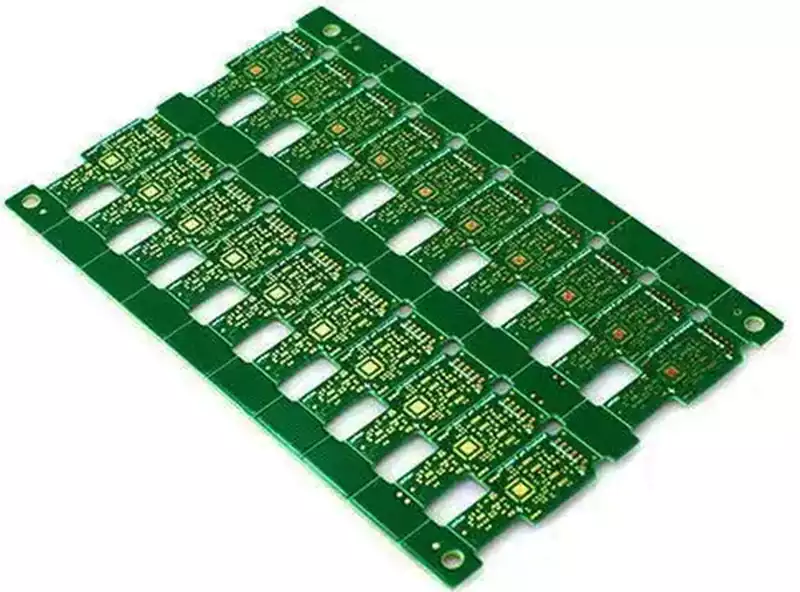
The choice of connection method directly impacts the quality of separated boards. For FR4 PCB panelization, the two commonly employed connection methods are V-Cut slot connections and stamped hole connections.
V-Cut slots are suitable for rectangular or regular-shaped boards, achieved by cutting V-shaped grooves between boards. The slot depth should be 1/3 to 1/2 of the panel thickness (e.g., 0.5–0.8mm for standard 1.6mm FR4 boards). The remaining connection thickness must be controlled between 0.6–0.8mm. This ensures the panel’s overall rigidity while allowing for easy breakage during subsequent separation, resulting in clean edges.
Stamp-hole connections are suitable for irregularly shaped boards or scenarios where V-cuts are impractical. These connections utilise uniformly distributed small holes (diameter 0.8–1.2mm) to link individual boards to the composite panel. The spacing between holes is 1.5–2mm, forming a ‘stamp-like’ connection structure.
The advantage of stamp-hole connections lies in their adaptability, preventing edge chipping during separation of irregular single boards. However, care must be taken to position the holes away from components and circuits, and any burrs remaining on the edges after separation must be cleaned.
The mechanical properties and heat resistance of FR4 substrate necessitate panel designs that specifically mitigate material weaknesses and enhance process adaptability. Although FR4 exhibits bending strength exceeding 300 MPa, its edge impact resistance is relatively low, making it prone to chipping during mass processing. Its typical glass transition temperature (Tg) of 130°C also leads to slight warping during reflow soldering. These characteristics must be prioritised in pcb panelization design considerations.
To counteract the tendency for chipping along FR4 edges,pcb panel designs must incorporate edge reinforcement measures. For thin FR4 panels with thicknesses below 1.0mm, reinforcement ribs should be added along the panel edges. These ribs should be 5-8mm wide and of the same thickness as the panel itself. They are connected to the single boards via V-cut slots and can be snapped off cleanly during separation. This approach enhances the overall rigidity of the panel assembly while preventing edge damage during transportation and processing.
For thick FR4 pcb panel assemblies exceeding 2.0mm in thickness, the angle and depth of V-cut slots must be optimised. Slot angles should be set between 30° and 45°, with slot depth controlled at one-third of the panel thickness. This prevents insufficient strength at connection points due to excessive slot depth, or separation difficulties caused by insufficient depth.
Addressing FR4’s susceptibility to thermal warping, PCB panelization design must optimise layout symmetry and heat dissipation uniformity. Layout must ensure the panel’s centre of gravity is centred and individual boards are symmetrically distributed to prevent thermal deformation during reflow soldering due to uneven weight distribution. Simultaneously, heat dissipation channels should be incorporated within the panel. For boards with dense component placement, the spacing between adjacent boards may be appropriately increased to 4-5mm to enhance heat dispersion during reflow soldering and reduce warping caused by excessive localised temperature differentials. Furthermore, for high-Tg FR4 (Tg ≥ 170°C) panelised PCBs, although exhibiting superior heat resistance, overall panel dimensions must still be controlled to prevent thermal stress concentration from excessive size. It is recommended that maximum dimensions for high-Tg FR4 pcb panels do not exceed 500mm × 500mm.
FR4 PCB panelization design must be optimised according to subsequent production process variations. Different SMT placement equipment, soldering techniques, and inspection methods impose significantly divergent requirements on panels. Precise adaptation to specific process scenarios maximises the efficiency advantages of panelised design.
For high-speed placement applications, panel design must prioritise enhanced positioning accuracy and layout regularity. High-speed placement machines achieve positioning accuracy of ±0.05mm, necessitating positioning hole tolerances not exceeding ±0.1mm. These holes must feature smooth inner walls free from burrs. Layout should employ regular matrix patterns with consistent spacing between boards to prevent placement efficiency losses from machine path adjustments caused by irregular layouts. Concurrently, the overall dimensions of the panel must precisely match the conveyor track width of the placement machine. The flatness tolerance of the track clamping section must not exceed 0.2mm to ensure stable panel conveyance.
For wave soldering applications, PCB panel design must optimise thermal dissipation structures and component protection. With wave soldering temperatures reaching 260°C, FR4 panel boards are prone to warping under high heat. Heat dissipation strips, 5mm wide and made from the same FR4 material as the panel board, should be added to the underside to enhance thermal efficiency. Furthermore, components positioned near the panel board edges must maintain a minimum 3mm clearance from the edge to prevent direct exposure to high-temperature solder vapour during welding, which could cause component damage. Moreover, the wave soldering process demands exceptional flatness from panel assemblies. Overall flatness deviation must be controlled within 0.5mm/m to prevent cold solder joints and missed soldering.
For AOI inspection scenarios, PCB panelization designs must incorporate dedicated inspection zones and reference marks. AOI inspection equipment relies on these reference marks for precise positioning; therefore, reference marks must be provided at the four corners and the centre of the panel. These marks shall be circular copper pads with a diameter of 1.5–2 mm, free from solder mask coverage on their surfaces, and with no components or circuitry within a 3 mm radius. Additionally, the panel must incorporate AOI inspection clearance zones to prevent component obstruction of the detection field, ensuring comprehensive defect detection of solder joints.
In actual production, numerous misconceptions in FR4 PCB panelization design can lead to reduced mass production efficiency and frequent quality issues. These errors often stem from insufficient understanding of FR4 material properties and manufacturing processes, necessitating careful avoidance.
Misconception 1: Excessive pursuit of space utilisation by reducing single-board spacing. Some designers reduce board spacing to below 1mm to minimise material waste. This causes chipping, debris shedding, and even damage to edge components and circuits during milling cutter processing. The correct approach is to adjust spacing based on FR4 thickness: for 1.6mm boards, spacing must not be less than 2.5mm; for 2.0mm boards, spacing must not be less than 3mm.
Misconception 2: Positioning holes too close to edges. Setting the centre-to-edge distance of positioning holes to less than 2mm causes cracking around these holes during pick-and-place machine gripping and transport, compromising positioning accuracy. The correct approach is to maintain a minimum centre-to-edge distance of 3mm. Where process edge width is constrained, elliptical positioning holes may be employed to enhance edge load-bearing capacity.
Misconception Three: Blindly employing V-cut slots for irregular single boards. For non-standard FR4 boards, forcibly using V-cut slots for separation may cause edge chipping, fractures, or even circuit damage. The correct approach involves selecting connection methods based on board geometry. Prioritise stamp holes for irregular boards, or incorporate transition connection blocks along irregular edges to enhance joint strength.
Misconception 4: Neglecting thermal stress dispersion in panelization. Excessively large panel dimensions (exceeding 600mm × 600mm) combined with asymmetrical layout cause uneven heating during reflow soldering, resulting in significant warping that compromises subsequent soldering quality. The correct approach is to limit maximum panel dimensions to 500mm × 600mm, ensuring centred mass distribution and symmetrical board placement during layout.
FR4 PCB panelization design must holistically consider material properties, process requirements, and production scenarios. Precise control over layout, connections, and thermal management is essential to avoid common pitfalls, thereby tangibly enhancing mass production efficiency and product quality.