Why are “Package Substrate” and “PCB” often confused?
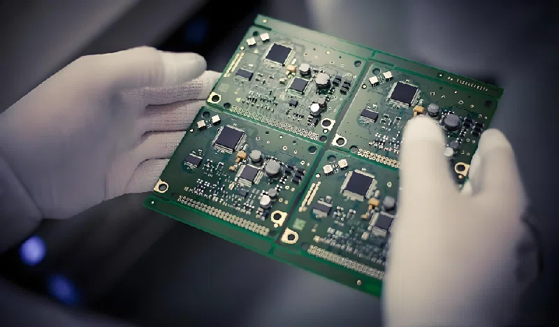
In the semiconductor and electronics manufacturing industry, “Package Substrate” and “PCB” are frequently discussed in the same context, and even used interchangeably in some non-professional settings. This confusion is not surprising, as they both appear to be circuit carriers composed of multiple layers of materials, and both serve the functions of electrical connection and mechanical support. However, they are fundamentally different in design logic, manufacturing precision, application level, and position in the industry chain.
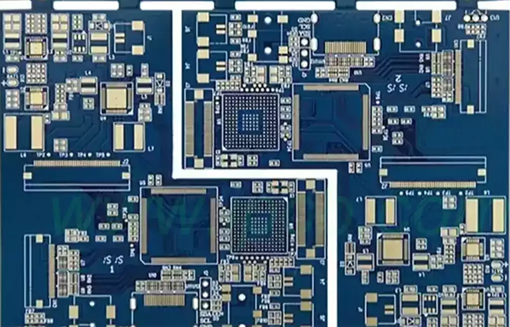
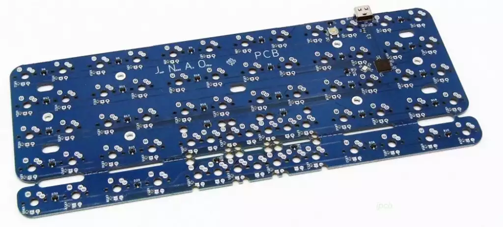
The core mission of a PCB is to complete the electrical connection between electronic components at the system level. It connects chips, passive components, connectors, and other functional modules, forming the “skeleton” of the entire electronic system. Therefore, PCBs focus more on signal integrity, power distribution, structural strength, and stability in mass production. In most electronic products, the PCB is a highly standardized, scalable, and fundamental component.
The role of a Package Substrate, on the other hand, is entirely different. It exists inside the chip package, acting as an “intermediate bridge” between the chip and the external PCB. At this level, circuit density has moved from the “millimeter level” to the “micrometer level.” The design goal is no longer simple connectivity, but rather how to reliably transmit high-speed, high-frequency, and high-power signals within extremely limited space. This also determines that the packaging substrate, from the outset, is not aimed at “universality,” but rather is a highly customized, key component tightly bound to specific chip designs.
From a functional perspective, PCBs address the complexity of electronic systems, while package substrates address the limits of the chip itself. As the number of chip I/Os continues to increase and process nodes continue to shrink, traditional packaging methods can no longer meet the demands, rapidly amplifying the importance of the packaging substrate. This is why, in fields such as advanced packaging, chiplets, and AI chips, package substrates are often considered a “bottleneck” link, while ordinary PCBs are rarely given such strategic importance.
Furthermore, the difference in manufacturing difficulty is equally significant. PCB manufacturing emphasizes yield, delivery time, and cost control; although line widths, spacing, and hole sizes are constantly shrinking, they still serve large-scale application scenarios. Package substrates, on the other hand, face the challenges of finer lines, higher inter-layer alignment precision, and stricter material stability requirements. Even minute deviations can directly impact chip performance or even cause failure. This difference determines the fundamental differences in equipment investment, material systems, and engineering capabilities between the two.
Therefore, “Package Substrate vs PCB” is not a simple comparison, but rather reflects the technological evolution of the electronics industry from system integration to chip-level integration. Understanding the differences between them is essentially understanding how modern electronic products are gradually approaching the limits of physics and technology.
Fundamental Differences in Structure and Design Logic
If the similarity in appearance is the most common reason for confusion between Package Substrate and PCB, then what truly differentiates them is their fundamental difference in structural design and design logic. Superficially, both are composed of multiple layers of dielectric and metal traces, but the answers to the question “why is it designed this way?” are almost completely opposite.
The structural design of a PCB primarily serves the integrity and manufacturability of system-level functions. At the overall system level, engineers need to consider component placement, signal routing, power integrity, and mechanical assembly space. The increase in the number of layers is often to achieve clearer routing partitioning, such as independent power and ground layers, or to provide a more stable reference plane for high-speed signals. Even with high-multilayer PCBs, the core of their structural complexity still revolves around “how to make the system work more stably and reliably.”
The design logic of a package substrate is completely different. It is not a “general-purpose circuit carrier,” but rather part of the chip packaging solution, its structure defined from the outset by the chip architecture. The chip’s I/O distribution, pad size, and signal type directly determine the layer stack-up and routing strategy of the package substrate. At this level, design is no longer “optimization,” but “adaptation”—every trace and every via serves a specific chip.
This difference is even more apparent from a trace scale perspective. While PCB trace width and spacing are constantly evolving towards finer details, they still need to balance manufacturing stability and cost control. Package substrates, on the other hand, must achieve high-density interconnection within an extremely small area, with trace dimensions often approaching the limits of manufacturing processes. This also means that the design of the package substrate itself must be highly tied to manufacturing capabilities, with almost no “buffer space” between design and process. The interlayer structure is another key difference between the two. In PCBs, layers are primarily functionally partitioned, with different signal types distributed hierarchically to reduce interference. In Package Substrate, however, the interlayer structure resembles a sophisticated three-dimensional network. The wiring density, dielectric thickness, and even copper foil characteristics of different layers directly affect signal delay, impedance matching, and heat conduction paths. This design complexity makes the package substrate’s structure itself part of the performance, not just a carrier.
Furthermore, PCB design emphasizes “replaceability” and “universal interfaces.” A single PCB can be compatible with components from different batches and sources to a certain extent. Package Substrate, on the other hand, lacks this flexibility. If the chip design changes, the package substrate often needs to be redesigned simultaneously. This strong binding relationship explains why the package substrate plays a highly sensitive role throughout the product lifecycle.
From a structural and design logic perspective, Package Substrate and PCB are not simply “higher or lower versions” of technological evolution, but rather two engineering solutions serving completely different levels of needs. The former pursues performance under extreme conditions, while the latter prioritizes stability and scalability in complex systems. This difference determines their irreplaceable nature within the entire electronics industry.
The Real Barriers Behind Manufacturing Processes and Yields
While the differences between Package Substrate and PCB are already apparent from the design drawings alone, the gap widens significantly once manufacturing begins. Manufacturing processes not only determine product feasibility but also directly dictate who can enter the field and who remains on the periphery.
The core challenge of PCB manufacturing lies in achieving stable mass production while maintaining electrical performance. This means the process must be highly repeatable and relatively tolerant of material and equipment compatibility requirements. Even in high-multilayer or high-frequency PCBs, yield can still be improved through mature process control, process redundancy, and testing methods. For PCB factories, yield management is more of a continuous optimization issue than a survival barrier.
The manufacturing logic for Package Substrate is entirely different. Due to its higher circuit density and more intricate structure, there is virtually no “tolerance for error” in the manufacturing process. Tiny alignment deviations and material performance fluctuations are amplified in the final product, directly affecting the chip’s electrical performance and even package reliability. This limits the manufacturing of package substrates from the outset to a very few manufacturers with advanced equipment and deep engineering expertise.
At the process level, package substrates often require more complex pattern transfer and multiple layer stacking processes. Each layer stacking, lamination, and circuit formation introduces new risks that cannot be mitigated by simple back-end repairs. A deviation in the front end can render the entire substrate unusable. This characteristic means that the yield of package substrates does not improve linearly but is highly dependent on the overall maturity of the process.
The impact of materials is equally significant. PCBs can adapt to different performance requirements through design adjustments within a wider range of material choices. However, package substrates have extremely high requirements for material consistency and stability. The thermal expansion characteristics, electrical properties, and long-term reliability of the dielectric material must be highly matched to the chip and package structure. Once a material is selected, it is difficult to replace it without affecting the overall design.
This high barrier to entry is also directly reflected in the industry structure. The PCB industry chain is relatively open, with numerous participants and constantly evolving but not concentrated technological approaches. The Package Substrate supply chain is highly concentrated, with extremely high barriers to entry. New entrants not only need substantial capital investment but also long-term accumulated process experience and customer trust. This is why, in the advanced packaging field, the packaging substrate often becomes a key factor limiting production capacity and technological advancement.
From a manufacturing and yield perspective, the difference between Package Substrate and PCB is essentially the difference between “precision manufacturing” and “mass manufacturing.” The former pursues stable output under extreme performance, while the latter pursues efficient replication in complex systems. This difference cannot be overcome by simple technological upgrades but rather by differences in the entire manufacturing system and engineering culture.
Divergence in Application Scenarios and Market Positioning
In practical applications, Package Substrate and PCB almost never appear on the same competitive dimension. They serve completely different product levels and address different decision-making logics. Understanding this differentiation helps clarify why these two types of products, despite their similar names, have almost no direct substitution relationship.
PCB applications cover almost all electronic systems, from consumer electronics to industrial control, communication equipment, and automotive electronics. Its value lies in “connectivity” and “integration”: combining disparate functional modules into a working system. Regardless of product complexity, the PCB remains an indispensable fundamental component of electronic systems, and its market demand is highly correlated with the overall scale of the end product.
In contrast, Package Substrate applications are more concentrated and closer to the chip. It primarily appears in high-performance processors, memory chips, network communication chips, and emerging advanced packaging solutions. In these scenarios, the package substrate’s purpose is not to connect more devices, but to enable the chip itself to achieve its designed performance. Without a suitable package substrate, even the most advanced chip architecture cannot operate stably.
From a market positioning perspective, PCBs emphasize versatility and economies of scale. Product update cycles are relatively flexible, allowing for rapid adjustments to specifications and designs based on end-user needs. When choosing a PCB, customers often seek a balance between performance, delivery time, and cost. Package Substrate, on the other hand, has almost no “universal models.” Each project is highly tied to a specific chip, resulting in long development cycles and high upfront investment, but once mass production begins, its lifecycle is often relatively stable.
This difference is also reflected in customer relationship models. PCB suppliers face a diverse customer base, and their order cycles are highly correlated with market fluctuations. Package substrate suppliers, on the other hand, tend to establish long-term collaborative relationships with chip design companies and packaging plants, participating in the product definition phase and even intervening in the design process before the chip architecture is fully finalized. This deep integration makes package substrate suppliers more like technology partners than simply component suppliers.
In terms of market size, the PCB market is massive but highly competitive with high price transparency; the package substrate market is relatively smaller but has higher technological concentration and barriers to entry. This is why, during semiconductor industry cycles, package substrates often exhibit different supply and demand characteristics than traditional PCBs.
From an application and market perspective, “package substrate vs. PCB” is not a matter of one replacing the other, but rather a natural division of labor at different levels of the industry chain. PCBs are responsible for building the breadth of electronic systems, while package substrates are responsible for supporting the depth of chip performance. Together, they drive the development of electronic products towards higher integration and higher performance.
Understanding the True Boundaries Between Package Substrate and PCB
Returning to the key phrase “package substrate vs PCB,” its value lies not in simply distinguishing between the two products, but in understanding how the modern electronics industry is evolving in layers. The difference between them is not a matter of technological superiority or inferiority, but a fundamental difference in their target audience and engineering goals.
PCBs, always viewed from the perspective of electronic systems, address how to achieve stable connections and functional integration in complex environments. They emphasize scalability, versatility, and cost control, forming the foundation for the rapid expansion of the electronics industry. Regardless of how end products change, PCBs exist in the supply chain with a highly adaptable approach.
Package substrates, on the other hand, are closer to the core of semiconductors. They do not pursue universality, but rather perfect matching; they do not emphasize flexible replacement, but rather performance release. Today, as chip performance approaches its physical limits, packaging substrates have transformed from “components” to “carriers of key technologies,” their importance no longer depending on quantity, but on indispensability.
From manufacturing barriers to market structure, from design logic to customer relationships, these two types of products have followed different development paths. PCBs represent continuous optimization within a mature manufacturing system, while Package Substrate represents the concentrated embodiment of high-precision engineering capabilities. Therefore, they do not compete on the same level, nor do they constitute a simple substitution relationship.
As electronic products continue to advance towards high performance, high integration, and high reliability, Package Substrate and PCB will continue to play irreplaceable roles in their respective ways. What truly matters is not comparing which is “more advanced,” but rather clearly defining their respective inviolable positions.