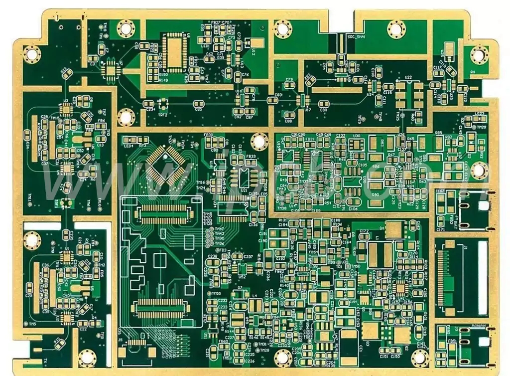
As one of the most widely adopted specifications in the industry, the cost-effectiveness and practicality of 4 layer PCBs are beyond question. However, achieving low noise floor hinges not on increasing layer count, but on meticulous control of stack-up logic, ground plane integrity, signal partitioning, and return paths. This article, grounded in practical PCB manufacturing scenarios and eschewing redundant exposition, deconstructs the logic behind achieving ultra-low noise within a 4-layer space. Drawing on mass production experience, it shares directly applicable stackup solutions and routing techniques, balancing technical rigour with accessibility. This empowers engineers to circumvent hidden pitfalls in design and production, achieving a balance between performance and cost.
Core Principles for Low Noise in 4 layer PCBs
Arbitrary stacking sequences neglecting power/ground layer proximity. Many engineers adopt a ‘top layer signals + second layer signals + third layer power + fourth layer ground’ structure for simplified routing. While seemingly convenient, this creates excessive distance between power and ground, causing power impedance to surge and rendering ripple noise ineffective to suppress. Simultaneously, signal crosstalk between the two signal layers creates dual interference, directly degrading signal-to-noise ratio.
Blindly segmenting ground planes, mistaking ‘segmentation’ for ‘isolation’. Some engineers physically divide ground planes on intermediate layers to distinguish analogue and digital grounds, seemingly isolating noise sources. This practice, however, severs signal return paths, forcing return currents to form large loops. Larger loop areas intensify radiated and received interference, elevate ground potential, and directly double baseline noise—proving counterproductive.
Signal routing lacks zoning, with analogue and digital signals intermingled. Placing analogue components with weak interference resistance—such as sensors and operational amplifiers—alongside digital noise sources like microcontrollers, clocks, and drivers, and routing them haphazardly, allows high-frequency noise from digital signals to couple into analogue signals. This compromises signal integrity, ultimately manifesting as elevated baseline noise and unstable performance—a common shortcoming in low-precision designs.
In fact, achieving ultra-low noise with a 4 layer PCB is logically straightforward: centred on a complete ground plane, tightly bonding power and ground layers, scientifically partitioning noise sources, and optimising return paths via shortest routes. This approach satisfies high-precision requirements without adding layers, representing the optimal balance between performance and cost.
Optimal Layer Stack for Ultra-Low Noise in 4 layer PCB
Top Layer (Layer 1) serves as the primary signal layer, prioritising placement of analogue small-signal components. As the core signal layer, it houses sensors, operational amplifiers, ADCs/DACs, crystal oscillators, and other analogue small-signal modules. These signals exhibit the weakest interference resistance and directly determine the lower limit of noise floor. Routing must adhere to the principle of ‘minimising distance from noise sources and reducing trace length’. Traces should lie flush against the underlying ground plane to maximise signal return path length, minimise radiation interference, and avoid unnecessary detours or vias.
Layer 2 comprises a continuous ground plane (GND), serving as the core for noise shielding and signal return. This layer is pivotal to the 4-layer low-noise design and must remain 100% continuous, with no slots, divisions, or breaks permitted. An unbroken ground plane provides the shortest return path for top-layer analogue signals, minimising signal radiation. It also acts as a natural shield, isolating top-layer analogue signals from interference with bottom-layer digital signals. This ensures uniform ground potential, prevents ground bounce noise, and establishes the foundation for low noise floor.
The third layer (Layer 3) constitutes the power supply layer (VCC), segmented as required without touching the ground plane. Positioned directly beneath the ground plane, it forms a natural parallel-plate capacitor. This configuration effectively reduces power impedance, filters high-frequency noise, stabilises chip power delivery, and minimises interference from power supply ripple to signals. Where multiple power supplies exist within the circuit (e.g., 3.3V digital power, 5V analogue power, ±12V supplies), segmentation occurs exclusively on this layer. Segmentation lines must bypass critical signal return paths, maintaining sufficient clearance between different power supplies to prevent sparking and noise coupling. Crucially, the continuity of the second layer ground plane must remain absolutely unaffected.
The fourth layer (Layer 4) constitutes the secondary signal layer, concentrating digital and noise-source signals. The bottom layer primarily houses digital components such as MCUs, FPGAs, interface chips, and driver circuits, alongside high-frequency noise sources like clock lines and PWM signal lines. Concentrating noise sources on the bottom layer—with no other signal layers beneath and a complete ground plane above for shielding—effectively minimises digital noise radiation. This prevents interference with top-layer analogue signals, achieving spatial noise isolation.
The core advantage of this stackup lies in its ability to achieve sub-100dB noise floor performance without adding extra layers, maintaining costs comparable to standard 4 layer pcb boards.This is accomplished through a ‘ground plane shielding + adjacent power/ground planes + signal zoning’ design, fully meeting high-precision application requirements. The solution also offers strong manufacturability, making it suitable for high-volume production.
Key Operational Considerations for Low-Noise 4 layer PCB
Implement strict partitioning to achieve physical isolation between analogue and digital domains. During layout, divide the PCB into analogue and digital zones. Concentrate top-layer analogue components in the analogue zone and bottom-layer digital components in the digital zone. Maintain a 5–10mm safety margin between zones. Prohibit analogue signals from traversing the digital zone and digital signals from entering the analogue zone. This isolates noise coupling at source and prevents cross-interference between signal types.
Adhere to the principles of ‘short, straight, thick, and close to ground’ for analogue small-signal routing. Minimise the length of analogue small-signal traces such as sensor outputs, operational amplifier inputs/outputs, and ADC sampling lines; avoid circuitous routing to reduce antenna effects. Prioritise straight paths; where turns are necessary, employ 45° angles to avoid signal reflections caused by 90° bends. Critical signal traces may be appropriately thickened (recommended ≥0.8mm) to reduce trace impedance. Maintain close proximity to the second layer ground plane throughout to ensure the shortest return path, minimising signal attenuation and interference.
Implement ground plane wrapping for noise source traces to isolate them and keep them distant from analogue zones. High-frequency noise sources on the bottom layer—such as clock lines, PWM lines, and driver lines—must be wrapped in ground planes during routing. Enclose signal lines with ground planes at intervals ≤0.3mm to minimise external radiation. Additionally, route noise sources away from the projected area of the top-layer analogue zone to prevent noise coupling into analogue signals via the ground plane, further reducing interference risks.
Prohibit routing across partition lines to ensure continuous return paths. Neither analogue nor digital signals must cross power partition lines or ground plane slots (except where special requirements necessitate pre-optimised return paths). Crossing partitions disrupts signal return paths, forcing currents to form large loops that instantaneously elevate noise floors. This represents the most easily overlooked yet critical issue in routing.
Place decoupling capacitors proximate to reduce power paths. Position decoupling capacitors (recommended 0402 or 0603 packages, with capacitance selected per chip requirements) immediately adjacent to each chip’s power pins. Limit routing lengths from capacitors to power pins and to ground to within 3mm, minimising the use of vias to ensure effective decoupling. This suppresses internal chip noise propagation and purifies the power environment.
Layer stacking and routing constitute ‘noise prevention’, while grounding and filtering represent ‘noise suppression’. Inadequate handling of either aspect renders even optimal layer stacking incapable of achieving ultra-low noise floors. Practical application must be prioritised to avoid excessive design.
Grounding design employs a ‘single-point common ground’ approach for analogue and digital grounds. Many engineers debate whether analogue and digital grounds should be separated. The correct approach is to share a complete ground plane on the second layer without physical division, implementing single-point connection only at the power input to establish a unified reference point. This ensures uniform ground potential while avoiding ground loops caused by multiple connection points, blocking noise crosstalk and balancing isolation effectiveness with signal stability.
The filtering design employs a multi-stage approach to purify the power supply environment. At the point where power enters the PCB, a multi-stage filter circuit is implemented: a 100μF electrolytic capacitor filters out low-frequency noise, while a 0.1μF ceramic capacitor filters high-frequency noise. Where necessary, ferrite beads or inductors are added to isolate noise between the pre- and post-stages of the power supply, ensuring the power entering the PCB is clean and free from interference. For analogue power supplies, additional RC filter circuits may be incorporated to further suppress power supply ripple, providing a stable power environment for analogue small-signal processing.
Achieving ultra-low noise in a 4 layer PCB is never a compromise through increased layer count, but rather the outcome of scientific design. The core lies in mastering three critical points: a complete ground plane forms the foundation, close coupling between power and ground layers is central, and signal zoning with optimised return paths is key.
The low-noise laminate and routing scheme for 4 layer PCB requires neither complex design techniques nor additional costs. It simultaneously fulfils high-precision, low-noise application requirements while maintaining mass-production feasibility, representing the PCB industry’s most cost-effective low-noise solution.